This thread has been locked.

If you have a related question, please click the "Ask a related question" button in the top right corner. The newly created question will be automatically linked to this question.

OPA548: OPA548 output impedance needed

Part Number: OPA548

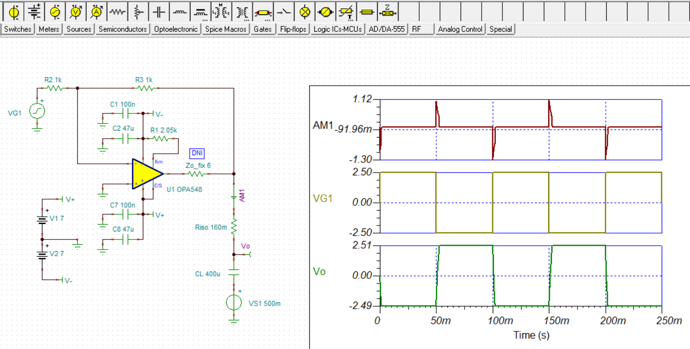
Need to know output impedance (Rout) for the OPA548?

The device is connected to a capacitive load and need to calculate the Pole and Zero of the output impedance according with the load.


Thx


Joe

  • Hello Joe,

    Please see the OPA548 Open-loop Output Impedance (Zo) vs frequency graph provided here:

    If you wish to run a Bode plot using Spice the OPA548 model Zo is a bit low. If you add a 6 Ohm resistance directly in series with the output, before the feedback return loop, that will shift the Zo curve up so that it better matches the graph. Do note that if your are trying to sink/source high current there will be a substantial voltage drop across the added resistor. I believe the model will allow you to bump up the supplies so that you can get the necessary output swing.

    However, for a stability analysis using a Bode plot the lightly loaded output condition is normally the worst case.

    Regards, Thomas

    Precision Amplifiers Applications Engineering

  • Thanks Thomas, 


    After reviewing the data, we'll trying  to source and sink about 1A with -2.4V output with 400uF of load capacitance. Can you recommend a possible solution?

    Joe

  • Hi Joe,

    I will need a bit more information before I would be able to determine if the OPA548 can provide this function.

    1. Is the output load purely capacitive i.e just the 400 uF load?
    2. How quickly must the OPA548 be able to charge the 400 uF capacitance? Remember i =C dv/dt
    3. What supply voltages are to be used to power the circuit?
    4. What gain will the OPA548 need to provide? Inverting or non-inverting?
    5. What are the input stimuli characteristics?

    Thanks, Thomas

    Precision Amplifiers Applications Engineering

  • Hi Thomas: 


      1. Is the output load purely capacitive i.e just the 400 uF load?

    The application has local decoupling capacitors on the gate which total 400uF.

      1. How quickly must the OPA548 be able to charge the 400 uF capacitance? Remember i =C dv/dt

    Slow, DC. The application has decoupling for the high frequency

      1. What supply voltages are to be used to power the circuit?

    +/-7Vdc

      1. What gain will the OPA548 need to provide? Inverting or non-inverting?

    Presently the gain is one, was thinking of making it two. Inverting.

      1. What are the input stimuli characteristics?

    +2.5Vdc, no AC component


    Some addition information:


    This would provide the -2.5V gate voltage to a depletion mode GaN device for a RF radar system application.

    To regulate the gate of the GAN JFET to -2.4Vdc, the gate current needs to be sourced and sunk, +0.5Vdc to -1Adc.  The RF device operates at 5GHz, the local decoupling capacitors provide the energy at that frequency.

  • Hi Joe,

    I put together a circuit based on your responses to my questions. I will need you to look it over to make sure I have implemented your responses correctly. You can see the resulting TINA circuit below.

    The OPA548 when in a non-inverting gain of -1 V/V and driving a pure 400 uF capacitive load results in a phase margin of about 1.7 degrees. That can cause sever transient overshoot, and the circuit is on the verge of oscillation. There is a second pole in the loop gain response that produces this behavior. The key to compensating for that second pole is to add a zero to the loop gain response at the appropriate frequency. It was determined that adding a 0.16 Ohm isolation resistor (Riso) in series with the output, outside the feedback loop, accomplishes that task. 

    The phase margin increases from 1.7 degrees to 76 degrees with the addition of this resistor. The circuit should be perfectly stable and as the simulation shows the output voltage shows little evidence of ringing. Since the output load is the 400 uF with the added 0.16 Ohm Riso the only time high output current flows is when the input voltage switches polarity. I used 100 ns rise/fall time for the input square wave, but the output waveform rise/fall time is limited by the OPA548 slew rate. That will affect how much the peak output current rises to.

    This can serve as a starting place and the circuit can be further optimized once you know all the final details for the application. The outcome provided here assures that the OPA548 can be compensated sufficiently when called upon to drive a 400 uF load and remain stable when doing so. If the customer's application cannot tolerate the small voltage drop that is developed across the 0.16 Ohm resistor, then there are other techniques to compensate the circuit.

    Regards, Thomas

    Precision Amplifiers Applications Engineering

    Here's the TINA file:

    OPA548_Vy_Lrg_C_03.TSC

  • Thanks Thomas.  Can a capacitor be placed in parallel with R3 to limit the bandwidth of the OP-AMP?


    Joe


  • Hi Joe,

    A capacitor can be added across R3 in the feedback loop and adding it will reduce the bandwidth of the amplifier, but it won't compensate the OPA548 when its driving the 400 uF load. Its the wrong ingredient when it comes to compensating the amplifier. The Riso would still be required to compensate the Op amp.

    I ran a separate simulation with a 1 uF capacitor across the feedback resistor and the 0.16 Ohm Riso still provided a high phase margin. Without the resistor the OPA548 will oscillate when driving the 400 uF load.

    Regards, Thomas

    Precision Amplifiers Applications Engineering