This thread has been locked.

If you have a related question, please click the "Ask a related question" button in the top right corner. The newly created question will be automatically linked to this question.

THS4551: THS4551 Analog Test Signals

Part Number: THS4551

We have designed custom PCB for video applications. In these PCB, we used THS4551 FDA to drive the ADC(AD9649). 

My question is related to the Test signals to fed THS4551 through function generator for Initial testing before integrating it in the system.

Input Requirement:

VIN+ = (0.9V ~ 4.3V)

VIN-=0.9V (Used as Offset)

Configurations:

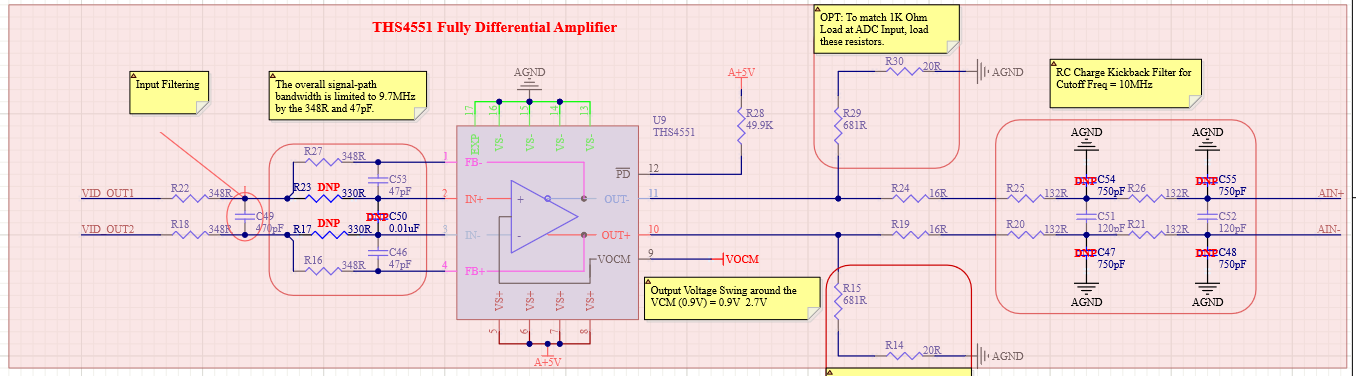
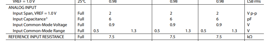
Schematics is attached for the VCM and Charge KickBack ciruicts.

Please provide the Test signals scheme to standalone test the FDA.

  • Morning Mohsin, 

    Let's discuss your ckt first. 

    Looking at the input side, 

    1. Those DNP 330ohm are shorts I am guessing, opens will open the DC feedback loop

    2. Assuming those are shorts, C49 is across the summing nodes - not an RC filter element then, but a noise gain shaping element with the 46pF feedbacks

    Best to start building a TINA sim to iterate on the ckt block before test issues discussed (what does the source look like? 

    The output filter is a simple cascaded first order sections? You can do better with a 2nd order RLC in terms of flatness to stopband transition if you would like. 

  • Dear Steffes,

    Thanks for the prompt reply.

    1. Yes 330 Ohm resistors are SHORT. I will replace them with 0Ohm jumper in the circuit.

    2. Thanks for clear me about the C49 as the Noise Gain Shaping element.

    3. I have simulated the circuit in TINA, but the results are not satisfactory. Please find the attached TINA model of the above circuit.

    Vocm = 0.9V;

    VIN+ = 0.9V ~ 2.1V (Desired Dynamic Range) which gives 2.1V - 0.9V = 1.2Vpp so the Output Voltage Swing will be 0.9 +/- 0.6V.

    VIN-= 0.9V (Fixed) Used for Offset 

    But the TINA Simulation didn't show the desired output. I have doing the Transient analysis.

    Please find the attached TINA model.

    Please help out in that.

    THS4551_RTM_Model_24122019.TSC

  • Anyway, your DC input side should be midpoint on the expected signal input range. Vg1 is a bit of an odd signal, you really wan that DC level at mid scale of your expected VG2 range - which you have set to 2.1. Here I just ran a DC operating point with the supplies changed to no clip. Which is was before. 

    but first, what does the ADC need, Well it is pretty forgiving on input Vcm voltage, I would shift that up to 1V to give more operating headroom in the THS4551. Also, it accepts a max 2Vpp differential - which is Vcm+/-0.5V - you are exceeding that right now, You can operate the FDA on 0 and 3.3V and get this work, but you need to attenuate your Vpp input to stay at about 1.9Vpp diff max. Also, add those ADC input impedance terms to your sim. 

  • Thank you so much for detailed description of Interfacing THS4551 with AD9649. All points are clear to me.

  • Dear Steffes,

    I have one question regarding the Vcm. We have to set the VCM according to the ADC, which should be 0.9V. Am i right in this sense? You have set it to 1V. 

    Can you please clarify this point.

  • All of these pipeline ADC's have a range on their input Vcm operating operating voltage. 

    The data sheet shows that where 0.9V is  a typical number, but it will accept the range that was in the spec table I inserted - using 1V, which is in range, will help the FDA operation