This thread has been locked.

If you have a related question, please click the "Ask a related question" button in the top right corner. The newly created question will be automatically linked to this question.

TLV9054: Amplifiers forum

Part Number: TLV9054
Other Parts Discussed in Thread: TLV4314, OPA4314, REF3325

Dear Sir,

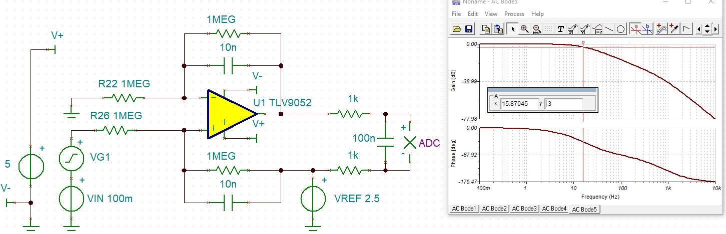
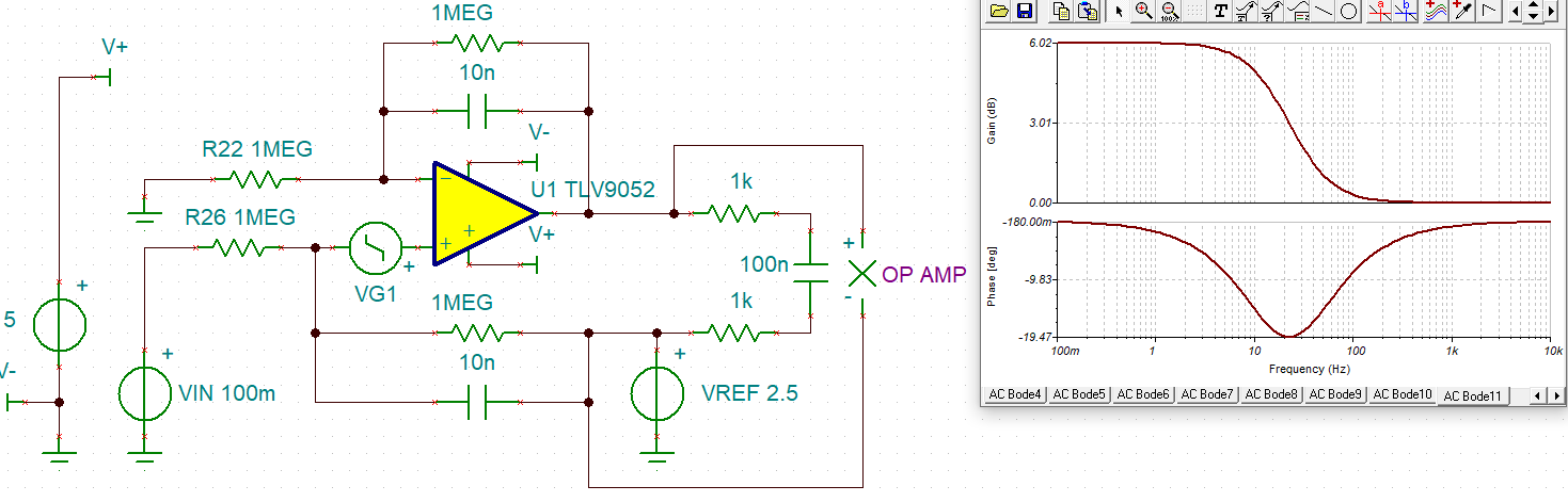
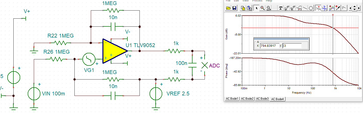
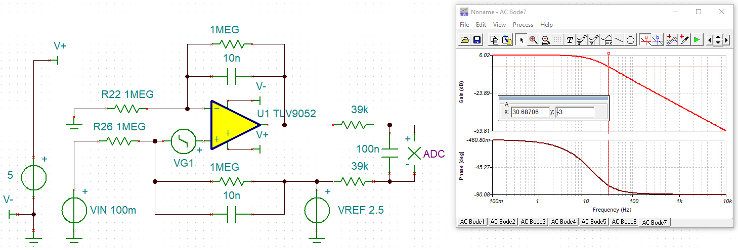
refer to attached file, it is my circuit for the front end of ADC.

I have request PTLV9054 and TLV9054 samples for this front end circuit. Please refer to attached picture for these 2 OPA.

test condition: CH0+-=100mV, ADC is calibrated by ADCMT 6156.

test result:

1. PTLV9054: ADC read 9999~10001. and the result is stable

2. TLV9054: ADC read 9995~10005. and the result is not stable.

7317.OPA.pdf

  • Hello Allen,

    Did I get the equivalent circuit right? What was the selection for the resistors? Were both tests with the same resistor setting?

    If the VIN was +100mV and 0mV (different than the schematic) then the "unstable" would be +/-50uV (noise) 

    How many TLV9054 have this observed behaviour? Does an ABA swap show that the behaviour follows a specific TLV9054?  https://training.ti.com/troubleshooting-tips-ic-b-swap

  • Dear Ron,

    All of the resistors are 1M for measuring 100mV.

    I have done A-B-A test.

    I made 2 PCBA. And they have the same problem.

    Then I change TLV9054  to PTLV9054. the read value is more stable.

    Becuase I only request 5 pcs PTLV9054. And I only have 2 good samples for this testing.

    thus, I can't do more A-B-A tests.

  • Dear Ron,

    refer to ADC read value, the noise is about 50uV @OPA is TLV9054.

    But I hope the read value varied < 20uV.

    the ADC has the digital filter and PGA inside. I set PGA gain=8 for measuring 100mV.

    As I tested 4 kind of OPA, I found that TLV4314 and PTLV9054 can meet my spec.

    OPA4314 and TLV9054 can't.

    Could you explain it?

    And what difference between PTLV9054 and TLV9054?

  • Allen,

    PTLV9054 and TLV9054 are the same other than the former was in pre production status. TLV4314 and OPA4314 will have the same expected noise level. I see that the application attenuates the high frequency input signal well (LPF = 16Hz) . -78dB at 10kHz

    [If pictures look blurry, click on them to open a clear version]

    [edited] However the op amp noise gain is amplified wide bandwidth and the square root of this bandwidth is significantly large especially because the op amps tested are wide bandwidth op amps. Noise gain starts at +6dB and it will drop to 0dB noise gain near 100Hz and hold 0dB gain past 1MHz.

    The post filter (1k 100nF 1k) is helpful but that LPF doesn't engage until 800Hz (-3dB) the noise gain is reduced to -22dB by 10kHz

    Changing the 1k resistors to 39k lowers the output LPF down to 20Hz. noise gain is -3dB at 31Hz and drops to -90dB at 10kHz. I expect about a 6:1 drop in output noise (due to op amp) from this resistor change. 

    The forward signal gain bandwidth does drop a little to 11.4 Hz from the resistor change. 10kHz gain is -180dB at 10kHz

    The resistor change will bring down the noise significantly. The DC error should not be an issue as long as the ADC doesn't draw a DC current.

  • Dear Ron,

    I don't think that the low pass filter issue.

    I have removed the capacitors(10n & 100n) and the result is the same.(not change bad and not change good)

    And when I change OPA, the read value of ADC is stable @ capacitors are removed.

    So I think if I(bias) or offset is drifted. Or open loop gain is drifted.

    P.S.

    I have use 1%  and 0.1% tolerance resistors for testing. the results are the same.

    Vref is supplied by REF3325AIDBZR

  • Allen,

    I see; there was no change with or without caps.

    Simulated total noise with caps.  Just 2uV total noise

    Simulated total noise without caps.  Now 957uV total noise

    In summary, changing the op amp with one that has different symbolization on the top but equivalent performance on the inside makes a difference (is it the same difference for 9054 and 4314?).  Therefore something other than the op amp also changed.  Removing the capacitors did not make a change therefore I believe that op amp internal noise is not the root cause.

    Revisiting the original observation "2. TLV9054: ADC read 9995~10005. and the result is not stable."

    Does the reading randomly move throughout that range or does it only occupy a small portion of the range?

  • it only occupy a small portion of the range.

  • Allen,

    I asked a colleague to take a look at this e2e thread to get a second perspective on this issue.  

  • Hi Allen,

    that the result was the same when you removed the 10n and 100n capacitors makes no sense to me.

    Can you give us an exact schematic of the circuit which was used during the noise measurement? Where comes the 100mV input voltage from? How is it referenced to the circuit? How does the REF3325 circuit look like?

    Have you kept in mind that the REF3325 also produces noise and that the analog switches can inject noise into the signal path via the control inputs and the supply voltage?

    Kai

  • Dear Kai,

    that the result was the same when you removed the 10n and 100n capacitors makes no sense to me. 

    -> Maybe the ADC has digital filter.

    Can you give us an exact schematic of the circuit which was used during the noise measurement?

    -> the noise can't be measured by my instruments. when I probe the OPA output, the read value of ADC will change. And the noise Vrms of  the different OPAs are similar.

    Where comes the 100mV input voltage from? 

    ->ADCMT 6146

    How does the REF3325 circuit look like?

    -> there are 1uF MLCC caps on the VIN and VOUT 

    Have you kept in mind that the REF3325 also produces noise and that the analog switches can inject noise into the signal path via the control inputs and the supply voltage?

    -> 1. I have change REF3325 to MAX6166. the results are the same.

         2. Because I can't measure the noise by my own instruments, I can't judge where the noise come from.

    below pictures are the schematic of VREF and PCB layout of OPA and ADC.

  • Hi Allen,

    Have you tried to look at the output voltage using a DMM without the output connected to the ADC? When you test this please make sure the output is completely disconnected from the input to the ADC?

    What is the sampling rate of the ADC? It is possible the op amp cannot drive the ADC at the sampling rate you are using. I recommend watching our TI Precision Lab Videos on SAR ADC Input Driver Design for more information on this.

    Thank you,

    Tim Claycomb

  • Hi

    The kind of ADC  is sigma-delta ADC. sampling rate < 100Hz when enable digital filter.

    There is the PGA in the ADC. So no driving issue for ADC.

    For 100mV measuring, the PGA gain setting is 8.

    So the ADC can get 800mV when input is 100mV.

  • Hi Allen,

    Thank you for the clarification. If you increase the input voltage such that the output of the PGA (input to the ADC) is Vref/2, do you still see the same issue?

    Thank you,

    Tim Claycomb

  • Hi Allen,

    now I understand why removing the caps might not have had an effect.

    Do you have a scope? Or can you borrow a scope from a friend?

    Kai

  • Allen,

    It may be time to leverage the 'science is repeatable' method.

    If needed order more samples for TLV9054, OPA4314 and TLV4314. Try these sample and see if only TLV4314 is a success or if a different result occurs. As much as possible try not to change the setup between tries.

    One new possibility is that AC line noise, 50Hz or 60Hz is the culprit and a minor change in setup affects how much AC mains voltage is on the ADC input (or the ADC reference voltage).

  • Hi,

    Maybe AC line noise.

    Because the power supply of my PCBA is from a isolated DC-DC module, and the DC-DC module input is from AC-DC power supply.

    when I use the DC-DC module without Y-cap, the noise is lower.

    If I use the DC-DC module with Y-cap(~200pF), the noise is higher.

    And when I connect ADC GND to AC GND, the noise will be lower.

    But at the same condition, the TLV4314 and PTLV9054 can get better result.

  • Hi Allen,

    DC DC converter, or "switcher" as I call them, are known to produce lots of ripple and noise. You might need consequent input and output low pass filtering directly at the switcher module to reduce the noise to an acceptable level. Because of that, I would prefer the use of a linear voltage regulator.

    Kai

  • Allen,

    It is not clear why TLV4314 and PTLV9054 are better. Of these two only TLV4314 is available. Would TLV3414 be a viable solution?

  • Dear Ron,

    I don't know why,too. TLV4314 is a viable solution. I want to try TLV9054, because it is cheaper and better spec.

  • Hi Allen,

    I'm pretty much sure that the switcher is your problem, not the OPAmp. Run a test and exchange the switcher by a linear voltage regulator.

    Kai

  • Allen,

    I understand your point of view. However, I have no further advice unless some new information provides a new clue.