Because of the Thanksgiving holiday in the U.S., TI E2E™ design support forum responses may be delayed from November 25 through December 2. Thank you for your patience.

This thread has been locked.

If you have a related question, please click the "Ask a related question" button in the top right corner. The newly created question will be automatically linked to this question.

INA180: Bidirectional output current?

Part Number: INA180
Other Parts Discussed in Thread: LM324, TINA-TI, INA181

Bidirectional output current from INA180?

In my design, I would like to offset the output of an INA180 with a resistive summing function.  For this to work correctly, the INA180 output would need to sink current (such as 1 mA or less) under some conditions.  An op amp such as LM324 can source or sink output current, but I see no mention of output current sinking capability in the INA180 datasheet.  Of course no amplifier is perfect.  I know that any output current variation will cause a small gain or offset error.  But let's say that changing the output load current (positive out of the amplifier) from -500 uA to -1 mA should not introduce much more error than changing the output load current from +500 uA to + 1 mA.

If the INA180 is not capable of sinking current without introducing significant error, I can design around this with an added op amp buffer or other means.  Can you please let me know?  

  • Hi Bob,

    can you show a schematic?

    Kai

  • Thank you, Kai


    In the attached PRELIMINARY schematic portion, U1 is my INA180A1 current sense amplifier.  Q16 emitter is connected to a 20V0 voltage reference. The current sense resistor is R49 (not shown but I label the connections to U1 pins 3 and 4.)  I want to turn on Q16 under some conditions to offset (increase) the divided output of U1.  This offset is intended to increase U4 output, thus indicating from U4 a higher output current than what is actually flowing.  Increasing the U4 output will cause my feedback loop (elsewhere) to reduce the actual output current.

     Under normal condtions with Q16 turned off the maximum expected output from U1 is 3V, corresponding to 6 Amps of output current.  But if actual output current is 0.5A and Q16 is turned on:

    U1 output should provide 0.5A * 0.025 ohms * 20V/V = 0.25V

    The Thevenin impedance of R3 and R54 is 8.33 K ohms.

    The Thevenin voltage sourced by R3 and R54 is 208.26 mV at U4 pin 3.Schematic section BobZ Feb 01 2020a.pdf

    If we assume 19.9V at Q16 collector, we have (19.9V - 208.26 mV = 19.69V) across (59K + 8.33K = 67.33K) so 292.5 uA through R91.

    The voltage at U4 pin 3 will be increased by (292.5 uA x 8.33K = 2.436V.)

    So the voltage at U4 pin 3 will be (2.436V + 208.26 mV = 2.644V)

    The voltage across R54 = 2.644 - 0.25 = 2.394V, so we have 239.4 uA flowing backwards into the output of U1.

    What will the output of U1 do under that condition?  Will it sink that current and remain at about 0.25V?

    I am having some difficulty to attach schematic.  Please let me know if I succeeded.

  • Hi Bob,

    yes, the schematic did come through.

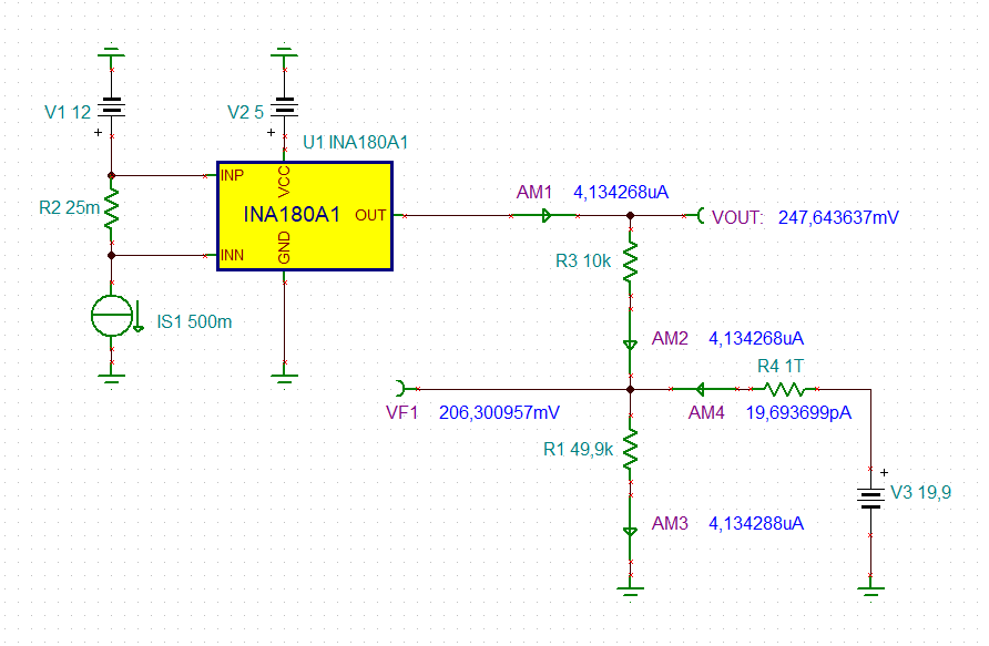
    The TINA-TI simulation says that it will work:

    By the way, that the output of INA180 cannot only source but also truly sink current can be seen from figure 19 of datasheet as well:

    Kai

  • Thank you very much, Kai.  To commit a pcb design to the INA180 this way, I am not certain that I would place that much trust in the simulation model.  However I certainly see your point with regard to Figure 19.  If I may, I would like to complain that Figure 19 should be clearer.  If I understand correctly, the upper and lower portions of Figure 19 actually are indicating opposite current directions.  I think that if the current polarityor directions were somehow labeled in this figure, I probably would have seen that and would not have initiated this inquiry.

    Anyway again thanks a lot for your help.  I think you have rescued the INA180 in my design.  I was thinking about going to an op-amp based current mirror in lieu of the INA180 but I think you have shown me that the INA180 will work OK.

    Best regards,

    Bob Zwicker

  • Hey Bob,

    We are happy that you could get your questions answered. You are correct that Figure 19 shows both sourcing and sinking current capabilities and the curves starting at 0V represent the sinking current. Figure 19 essentially shows you want to keep the output current of INA180 within +/-5mA for best dynamic range. Best practice is to limit it within +/-1mA. If the INA180 is trying to sink 27mA, then the output voltage will not be able to go below 1V. If INA180 is trying to source 5mA, then the output cannot go past approximately {Vs-0.3V}.

    Adding a buffer to the output will definitely increase the output current range if necessary.

    Another I possible idea is to use the INA181 and an op amp to convert the INA181 into a current-output device as opposed to voltage. Doing this allows you to easily pull-up the output to a desired voltage. See section 5.3, Figure 17 of the following application note:

    http://www.ti.com/lit/an/slya047/slya047.pdf

    http://www.ti.com/lit/an/sboa358/sboa358.pdf

    Please post back with your questions.

    Best,

    Peter

  • Ahh.....that is interesting.  Reminds me of a current mirror.  I will be mainly using the INA180 output into an error amplifier and a comparator; I see no problem with an output of less than 4V and 500 uA into a ground referenced resistive load.

    Thanks a lot.