This thread has been locked.

If you have a related question, please click the "Ask a related question" button in the top right corner. The newly created question will be automatically linked to this question.

THS4551: How to achieve the highest signal to noise ratio for a high gain (G = 50) 16 bit ADC application.

Part Number: THS4551
Other Parts Discussed in Thread: THS4541, THS4561

Hello,

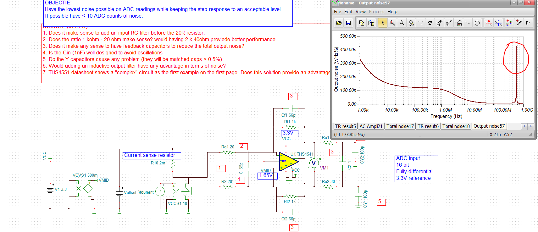
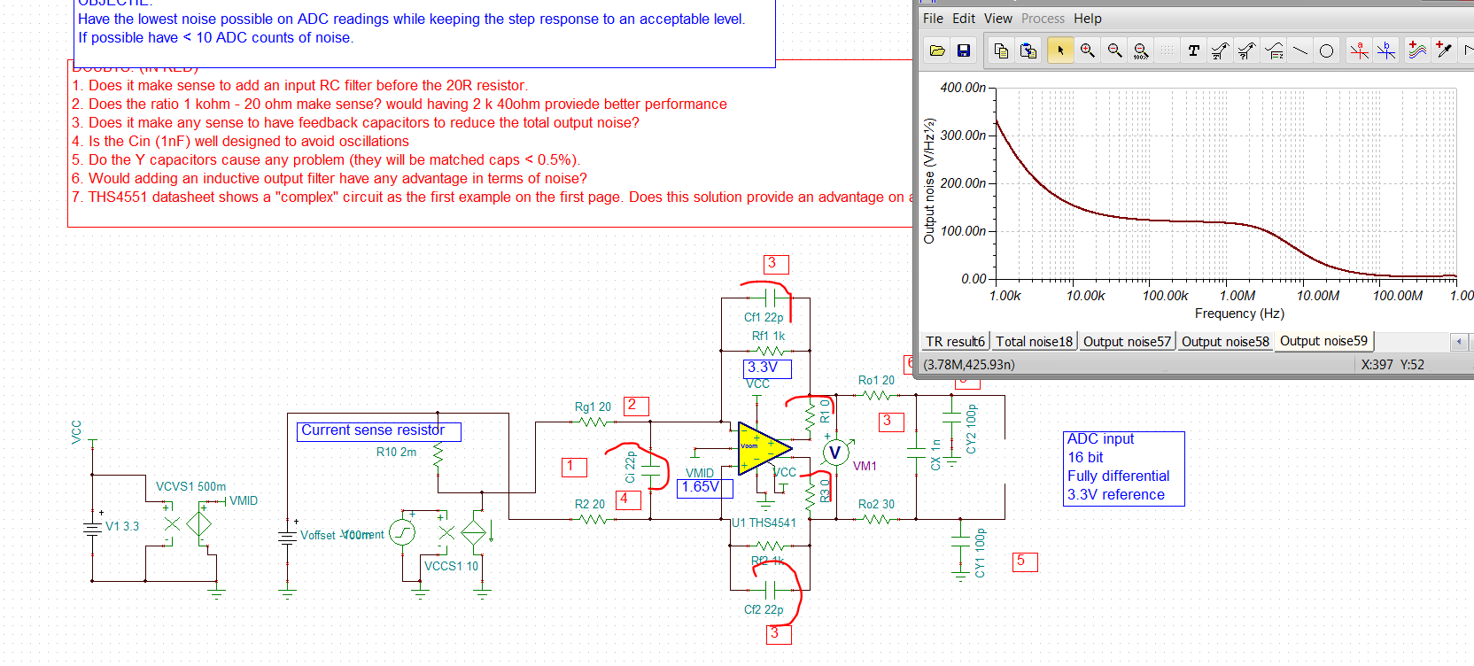
I am using THS4551 as a current sense amplifier and we would like to achieve a high signal to noise ratio while keeping bandwidth and step response to good levels. 

We would like to have your feedback on the circuit topology and solve some of our doubts. Attached is the TINA simulation we are using. 

CIRCUIT BACKGROUND AND FUNCTIONALITY:
THS4551 is used as a current sense amplifier.
The input signal has a maximum differential amplitude of ±66 mV. Common mode < ±100 mV
The gain must be around 50 to have a full differential output range of ±3.3V that goes directly to a 16 bit ADC. 
Step response to 95% must be between 125 ns (WISH) to 500 ns (MUST). This is why we do not use dedicated INAxxx current sense amplifiers.

OBJECTIVE: 
Have the lowest possible noise on ADC readings while keeping the step response to an acceptable level. 
If possible have < 10 ADC counts of noise. ~ 100 µV RMS differential.

QUESTIONS (also inside TINA file):

1. Does it make sense to add an input RC filter before the 20Ω resistor?  
2. Does the ratio 1 kΩ (feedaback) - 20 Ω make sense? would having 2 k 40 Ω  provide better performance. Power consumption is NOT critical here. 
3. Does it make any sense to have feedback capacitors to reduce the total output noise?
4. Is the Cin (1nF) well designed to avoid oscillations.
5. Do the Y output capacitors cause any problem (they will be matched caps < 0.5%).
6. Would adding an inductive output filter have any advantage in terms of noise?
7. THS4551 datasheet shows a "complex" circuit as the first example on the first page. Would that solution provide an advantage on an application like ours?

THS4551_TRANSIENT.TSC

  • Ernest, congratulations on possibly the best framed question I have seen here. I will start looking at it with my FDA noise analysis tools, might take a bit. 

  • Also Ernest, I am working with your file now - it is also fortunate you are using the original July2016 TINA model I worked on - it models the differential amp noise correctly (but not the CM noise, finishing up an article on that right now). The new 2019 THS4551 model tested out to not be producing the noise correctly - that might get fixed, but continue with the 2016 model for now - 

  • Incidentally, your question 7 about the front page circuit I put there - that is an MFB filter with stabiity and post RC elements added. I was getting a great deal of MFB filter design questions at the time on early design ins. It is more complex but might incremently reduce your integrated noise having a steeper rolloff - do you care too much about complexity? 

    Your 125nsec settling to 5% might be a little demanding - if we take the typical 0.35/F-3dB rise time to get betwen 10 and 90% and double that get well within 95% that leads to about 5MHz target? using the 135MHz GBP in the THS4551 at noise gain of 51 is only 2.6MHz. So you should perhaps expect more like a 250nsec settling inside of 5%. Your design is currently has an interesting piecewise linear waveform? I ran you sim, zoomed in a one of the 0 to1V steps and see about 400nsec to 95%. Probably could boost your current 1.3MHz BW up a bit to get some settling margin, which will integrate more noise - that's where maybe a little more agressive filtering might come in handy. I will maybe shoot for something like 1.8Mhz

  • Hi Michael,

    thank you for your feedback and answers! Regarding the MFB filter, 14x 0402 passives may be ok. My main concerns would be the circuit's physical size and layout. The circuit is inside a dense power board and I don't like big areas that can be more vulnerable to EM fields. 

    Regarding 125 ns 5% I agree it is very demanding. Let's focus on a 250 ns to 400 ns target and the < 100 µV rms output noise objective.

    Looking forward to your suggestions. 

    Ernest 

  • I think you are going to need a lower voltage noise device, like the THS4541, 

    THS4551 current sense simulations.docx

  • Hi Michael,

    thank you for your quality responses and doc. I have updated the simulation with THS4541, attached, looks promising.

    Could you help me optimize the signal to noise with this amplifier? Also do you think it is necessary to consider the MFB filter?

    Thanks again,

    Ernest

    THS4541_TRANSIENT.TSC

  • Yes the THS4541 is better, 

    1. overall BW is about 1.6Mhz, about as low as you can go and get <500nsec

    2. with the lower voltage noise, the resistor noise was now a meaningful part with 2kohm feedback, changed that back to 1kohm, 

    3. The integrated noise is still 168uVrms, well over your 100uVrms target

    Here is the circuit so far

    4. Your transient sim shows within 95% in 300nsec and final value in 500nsec. If indeed that 95% is the target, you could slow this down a bit - that will integrate less noise, 

    I went on at this point to do two passes of 3rd order filter, could not get the noise lower than above, so probably not worth it. 

    3rd order Bessel gain of 50 with THS4541.docx

    Here is the 1.2Mhz 3rd order file, 

    THS4541_updated version 1.2MHz Bessel.TSC

  • Incidentally Ernest, I went on to run the simple RC pole one with 1kohm feedback and 20ohm inputs with the ADA4930, that is the lowest voltage noise and yes it shows integrated noise of 77uV, below your target - but it does pull an extreme 35mA supply current but will operate on 3.3V supply. I have not validated its noise model yet which would be prudent. 

  • Hi Michael,

    thanks for the proposal. I think that the first-order solution provides the best tradeoff between step response and noise. The results I get are far better than with THS4551 so I will proceed to the layout.

    Some last doubts:

    • Based on your experience, do you think the output capacitors (Y) to GND (100 pF) can improve the ADC noise?
    • I guess the feedback capacitors should be tightly matched (<2%) to provide their desired effect right?

    THS4541_TRANSIENT_1storder.TSC

    Although 

  • So the effect of the 100pF to ground are to filter output common mode noise. There is also some interaction with the sampling event in the ADC (you have never mentioned that, but it will often have its on internal RC network that you might want to add to the sims). 

    FDA output common mode noise does not appear to be well modelled but is often measured - sometimes correctly, sometimes not. The point I make in this upcoming article is since it is not modelled, plan on driving the Vocm pin ( do not let it float) with a lower noise source to remove it. 

    I don't think it hurts to have those to ground, you can eventually try removing them and see what your system level performance becomes. 

    Recently, in some other active filter discussions we have found that 1% C0G caps are actually really cheap these days - just use those and you should be fine. 

  • Thank you Michael for your help! I would let you know if an issue appears with the best simulator... the real board. :)

    Ernest

  • Ooops!!

    So an important check is phase margin - the quickest way to see if you have issues is to look at spot noise at the output pins before the RC filter, omg - this is oscillating, 

    That is always a concern with these real fast RR out stages into a feedback cap. I got into that in a couple of articles,

    This one sets up the method, 

    https://www.planetanalog.com/stability-issues-for-high-speed-amplifiers-introductory-background-and-improved-analysis-insight-5/#

    This one looks at FDA's with that reactive open loopoutput impedance in the model (and part). 

    https://www.planetanalog.com/stability-issues-and-resolutions-for-high-speed-fully-differential-amplifiers-fdas-insight-8/

    Without setting up the LG sim, here I added 20ohm inside the loop to isolate this effect, This works well - I always wondered if we should have put something like that on chip in the output lines - trying to market RR output into a load gets harder if you do - 

  • And then back to the output CM noise issue, 

    I was focused in on going down to 2Hz without issues - the worst is if you float the Vocm pin to get the default internal mid supply - very erratic reporting, here is the table for the article - I was trying to pull off the 100Hz numbers - what sim testing I have done shows this is not in the model correctly. The THS4561 plot of floated CM noise is likely incorrect, 

  • Hi,

    In my design, I have 22 pF feedback capacitors wich leave to a nice step response. With this value, the peak resonance is not observed even without those 20Ω resistors. I did a quick check with 30 pF and still not resonating. For layout, I would like to avoid the 20 Ω additional resistors, do you thing it is a safe bet to trust the simulation model on this?

    Thanks,

    Ernest

  • Yes, that looks ok - in theory you should run a LG PM sim to see where you are out there in the 700Mhz region.Normally I am ok with 30dg or more, 20 to 30deg start to get a little nervous, <20deg - should work on it. 

    I certainly understand your desire to not have those inside the loop resistors. One concern I saw in other designs is what if someone years later comes along and boosts those feedback capacitors thinking there is no stability interaction - and you start shipping oscillators. You could document that.