This thread has been locked.

If you have a related question, please click the "Ask a related question" button in the top right corner. The newly created question will be automatically linked to this question.

THS4509: THS4509 to ADS42LB69 DC coupled input

Expert 1760 points
Part Number: THS4509
Other Parts Discussed in Thread: ADS42LB69, THS4541

Hello,

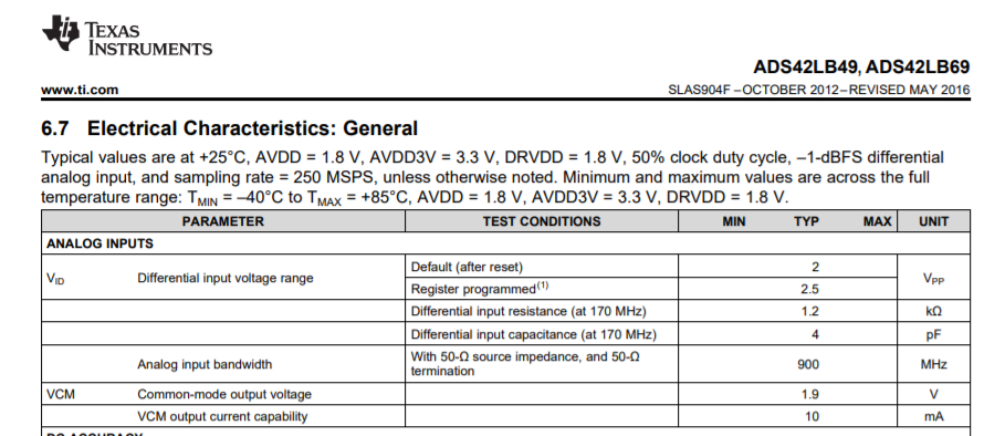
        Please advise on a DC coupled input circuit using the THS4509 and the ADS42LB69. Is it possible in the first place (because the ADC has a common mode input voltage)?

Regards,

  • Well Certainly SM, that is what FDA's are for, simply tie the CM output of the ADC with an RC filter to the CM control input of the FDA, This ADC has a relatively high CM so the 2Vpp input range will be easily supported by the THS4509 

    However, a more recent part you might look at is the THS4541 which has DC coupled ADC driver examples in its datasheet. 

  • Hello Michael,

             Thank you for the super quick answer (just curious it must quite early there!)

    Will look into the device, I am assuming the THS4509 and 4541are pin compatible. A quick question, how do I estimate the current consumption of the FDA in different configurations when connected to the ADC (example with no signal (quiscent current?), with a signal of a particular level etc). 

    The reason for asking this is to decide the power supply configuration (hence to know the maximum current that will be drawn by the op-amps). 

    For an AC-coupled input, I have attached my TI simulation file. It is configured for V+ = 5V and V- = GND while connected to the ADS42LB69. Please advise if V+ can be made 3.3V? 

    Thanks again,

    Example_29Dec16_ADCinput_forscreencapture.TSC

  • Ohyes, it is really early, like 2:30AM, 

    Your circuit simulates ok, couple of comments, 

    1. your upper RC networks to ground should match what is on the lower side - 

    2. Normally you put some extrinsic C across the ADC inputs instead of just parasitic, for instance maybe 10pF reducing the series Rs from 100ohm to 33.2ohm gives the same response shape - this is intended to absorb the sampling edge. 

    3. Here is a table of I/O swing limits, you can use these to test operation at 3.3V supply with 1.9V cm and +/-0.5V max on each output pin. Might be close on the THS4509, but the THS4541 should be fine, The maximum output excursions are 1.4V to 2.4 around 1.9Vcm. The output headroom on the THS4509 is 1.1V so on 3.3V supply it would clip. The RRout THS4541 would not. 

  • Here is your ckt with a few adjustments and THS4541 substituted on 3.3V supply

    1. I added the series 49.9ohm and changed the blocking cap to match the two RC on the top side

    2. I added a 10pF external diff cap at ADC and dropped the R's to 33.2ohm

    3. dropped supply to 3.3V

    AC response is 6dB lower due to input matching loss, but same BW. 

    Example THS4541 ADC driver.TSC