This thread has been locked.
If you have a related question, please click the "Ask a related question" button in the top right corner. The newly created question will be automatically linked to this question.
Hi team,
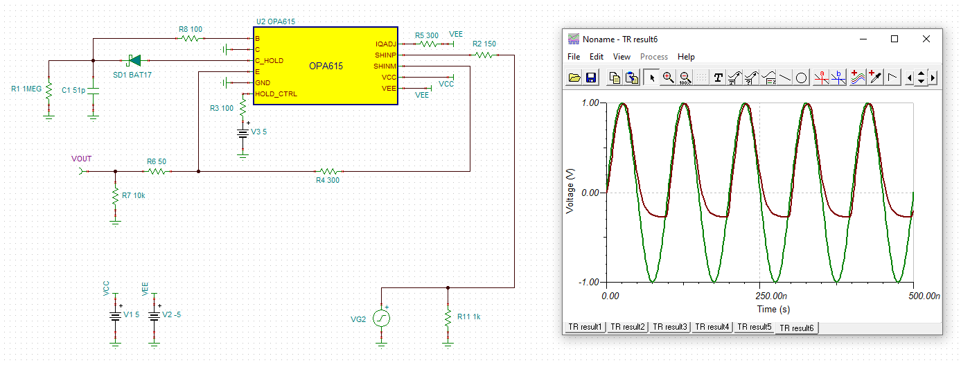
My customer found a problem using OPA615IDR. The schematic diagram of OPA615IDR is as follows:
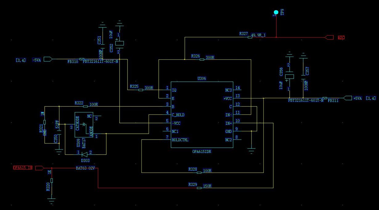
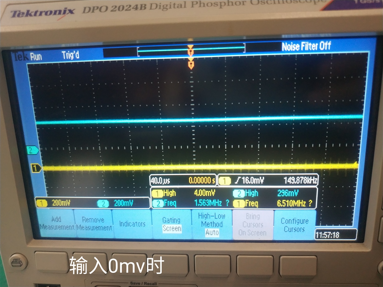
When OPA615_IN network is suspended, after ± 5V voltage is applied, some OPA615 chips can measure about 45mv DC level on ADC network. In my opinion, under normal circumstances, when pin10 of OPA615 is input 0V, Pin2 output 0V is normal. Is that right ?
Cross experiment: the chip on the normal board is welded to the abnormal board, and the abnormal board becomes normal; the chip removed from the abnormal board is welded on the normal board, and the normal board becomes abnormal. The chip was purchased on TI store. Is this caused by chip differences? Could you give any suggestions
Hello Amy,
I don't believe the offset at the emitter should be as high as it is, however there is also no input offset voltage spec for the SOTA in the datasheet. Would you be able to measure the voltages at pins 10 & 11 & 2 of both normal and abnormal devices?
Best,
Hasan Babiker
Hi Hasan Babiker,
Thanks for your response. The voltage of each pin is shown in the table below
OPA615 pins value |
normal |
abnormal |
Pin2 |
0mV |
42mV |
Pin3 |
0mV |
42mV |
Pin4 |
107mV |
-4.24V |
Pin5 |
-4.88V |
-4.88V |
Pin10 |
0mV |
0mV |
Pin11 |
0mV |
42mV |
ADC network |
0mV |
42mV |
Hi Amy,
I'm sorry, but this circuit makes no sense to me:
What is the purpose of this circuit?
Kai
Hello Amy,
Surprised to see that pin 4 is being driven down to -4.24V for pin 4, device maybe damaged. Is this the only unit that is showing this type of response?
Best,
Hasan Babiker
Hi Kai,
Thanks for your response.
But the customer feedback said that this circuit test is OK, the following is the customer test waveform
Because when the input of this circuit is 0, the output is about 40 ~ 200mV DC level, so the circuit can only detect the peak voltage of input > 200mV
Hello Hasan,
The customer tested a total of nine chips, five of which were abnormal.
What is the cause? Is the circuit designed correctly? Will soldering cause this problem
Hi Amy,
something is wrong in the schematic you showed in the original post. Why are there two Schottky diodes, U309 and D303, in parallel? And how shall this circuit be able to perform a bipolar peak detection? Even if only an unipolar peak detection is desired the circuit as shown in the schematic will not work because another Schottky diode to signal ground is missing.
Can you please show an updated schematic? :-)
Kai
Hello Amy,
I agree the parallel diodes here isn't clear to me as well. There was also an addition of a 1k-ohm resistor for R321 that isn't in the "Fast Bipolar Peak Detector" circuit in the OPA615 datasheet.
Best,
Hasan Babiker
Hi Amy,
the scope plots show a rather low frequency of about 50kHz. In this frequency range a peak detector using standard OPAmps might be a better choice :-)
What is the customer wanting to do? Can you elaborate a bit, please?
Kai