This thread has been locked.

If you have a related question, please click the "Ask a related question" button in the top right corner. The newly created question will be automatically linked to this question.

LMH6517: LMH6517 SPI operation trouble

Part Number: LMH6517

Hello,

I put the LM6517 in a board of my own design and the SPI reading and writing don’t work. I configured the chip in SPI with the MOD0 connected to ground and MOD1 floating. I put the schematic below. I originally had 5V on some digital inputs, so I used a fresh board and cut the traces by hand.

For pin 1, I considered the big dot under the markings. Is this the proper orientation for pin 1??? Can somebody please post a clear picture of the eval board zoomed in on the chip???  I put a picture of the PCB. I labelled in red the SPI signal names.

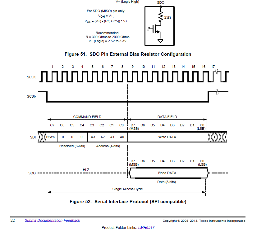
The datasheet says on page 22 to put a 300 ohm to 2k ohm resistor pull up to 3.3V. I put a 1.8k resistor on SDO once as a pull down to ground and once as a pull up to 3.3V. The SDO never drove the resistor at all in either way.

I plugged my board temporarily to an Arduino M0 Pro with Cortex M0 processor with full ARM debugging. I use hardware SPI.

I tried sending a few different values for the gain. I am not too confident for my transformer circuit that seems to be shorting out the function generator. That will go into another post.

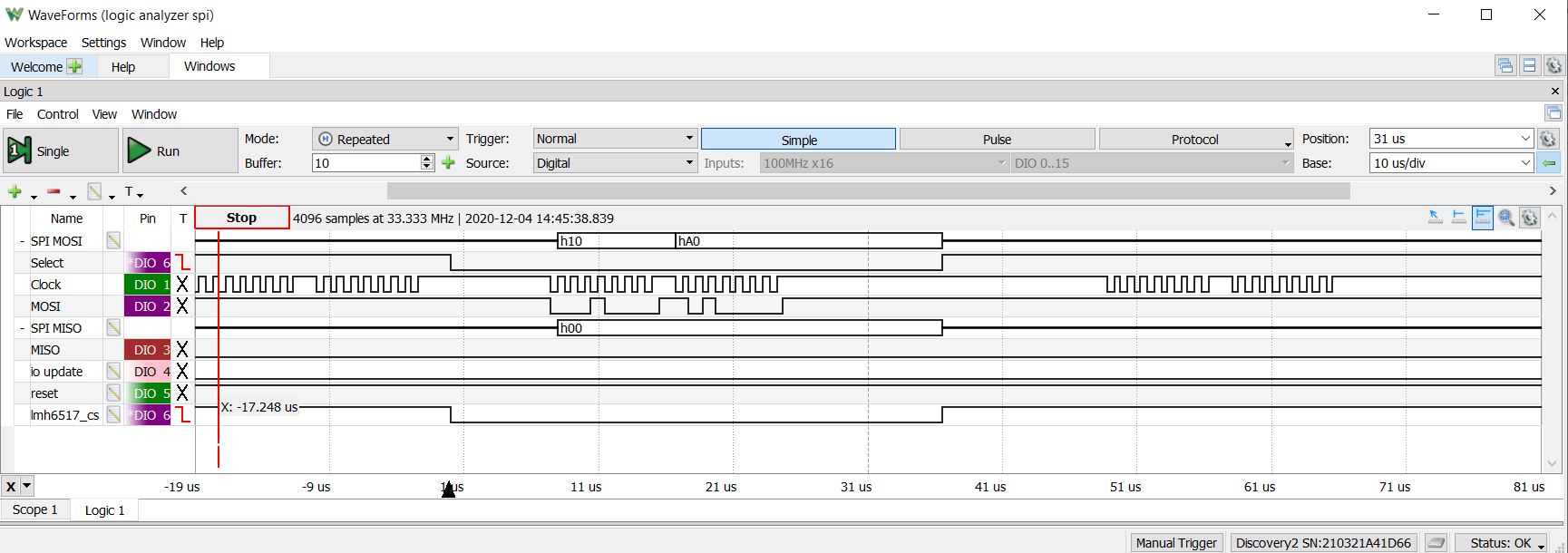
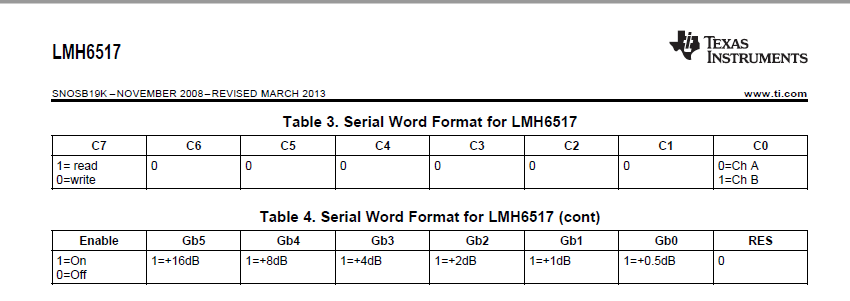
I tried issuing a read command in mode 0 with 1MHz clock. I lower CS, send 0x80 and send one more time x80 as a dummy byte while I read. Next, I raise CS. The LMH6517 is not driving SDO. It stays high. I attached my logic analyzer capture and my Arduino code. For reference I put captures of the LMH617 datasheet relevant to the timing.

Does anyone see something wrong?


#include <Arduino.h>

#include <Wire.h>
#include <SPI.h>

const int slaveSelectPinLmh6517 = 8;
const int slaveSelectPinAd9958 = 5;

void lmh6517RegularRead(){
  volatile uint8_t instruction = B10000000; /*read for channel 0*/
  volatile uint8_t value1;

  digitalWrite(slaveSelectPinLmh6517, LOW);
  delayMicroseconds(5);
  SPI.transfer(instruction);
  value1 = SPI.transfer(instruction);
  delayMicroseconds(5);
  digitalWrite(slaveSelectPinLmh6517, HIGH);
  delayMicroseconds(10);

  Serial.print(instruction);
  Serial.print(',');
  Serial.println(value1); 
}

void lmh6517RegularWrite(uint8_t gainCode){
  volatile uint8_t instruction = B00000000; /* Write to channel 0*/

  digitalWrite(slaveSelectPinLmh6517, LOW);
  delayMicroseconds(5);
  SPI.transfer(instruction);
  SPI.transfer(gainCode);
  delayMicroseconds(5);
  digitalWrite(slaveSelectPinLmh6517, HIGH);
  delayMicroseconds(10);
  
}

void setup() {
  Serial.begin(9600);
  Serial.println("start");
  pinMode(slaveSelectPinAd9958, OUTPUT);
  pinMode(slaveSelectPinLmh6517, OUTPUT);

  digitalWrite(slaveSelectPinAd9958, HIGH); 
  digitalWrite(slaveSelectPinLmh6517, HIGH); 

  SPI.begin();
  SPI.setDataMode(SPI_MODE0) ; 
  SPI.setBitOrder( MSBFIRST);
  SPI.setClockDivider(48) ;
}

void loop() {
  lmh6517RegularWrite(0xF0);
  lmh6517RegularRead();

  delayMicroseconds(200);
}

Thanks,

Frank


  • Hello Frank,

      I will look into this issue, and get back to you by tomorrow.

    Thank you,
    Sima

  • Hello Sima,

    Thanks for looking into this. I made some more measurements.  The LMH6517 seems to be stuck in a gain of approx 10. I can't get it to respond to any SPI command to change the gain or to shut off the output

    I used the schematic from the eval board to design the analog input. I don't have the eval board. I took a  minicircuit TC4-1W+ transformer where I placed a 0.2Vpp 3MHz signal on the primary.On the primary, I have one side at DC, while I excite the other side. At the secondary output, I get 0.2Vpp on each single ended side, so 0.4Vpp double ended. I verified that both single ended outputs of the transformer are opposite polarity.  I see that the signal propagates through the LMH6517 with an internal gain of 10.

    Do you have any information on what is the default at power up for the gain and the enable/disable ??

    Frank

  • On the bottom of page 4 of the datasheet, it says Inter-access gap: minimum time serial chip select pin must be asserted between accesses. What's that about??? I just changed my code. After doing a lower CS, transfer bytes, raise CS, I just added a dummy transfer of one more byte. That makes extra clock cycles with CS high. There is no change.

    Frank

  • Hello Frank,

      I have attached a word document I wrote while reviewing your questions and reading through the product datasheet. I am a bit confused on the gap between the two sections of 8 Clk cycles. Would you be able to explain that to me? 

      For your write command, it seems like your obtaining the correct gain value. You are sending a write command to CHA at max gain (on page 3 of the datasheet the max gain is around 22dB or 10V/V) which is 0x80 going by tables 3 and 4 in the datasheet. For your read command, you are sending the incorrect word format. In this case, you are still sending a write command to CHA at max gain. The CS is an assertion for any type of command (read or write). As you have done correctly, you have asserted CS for the 1st CLK cycle , then de-asserted it after the 16th. For the second command, you would have to wait three CLK cycles before asserting CS again. This then follows the same pattern as before, but you can send a different type of command on SDI. 

      As a test, would you be able to send a write command to CHA for a minimum gain of -9.5dB or 0.335 V/V: 0xFE. Wait three CLK cycles before asserting CS, then sending a read command to CHA: 0x8080. 

      Let me know if you have any questions written on anything in the word document as well.

    LMH6517.docx

    Thank you,

    Sima

  • Hello Sima,

    Thanks for your email. All of you at TI are really really helpful.

    I made some progress. I did not make the read work. I have some more questions for you. I will come back to that at the bottom of this message.

     WRITE

    I managed to write to channel 0. I did not make it work with the command field bits provided in the data sheet. I made the write work by sending 0x10 in the command field. It also seems to work with sending 0x30, 0x50 and also 0x70. I could not make the write to channel 0 work with 0x00 in the command field. The command field seems to behave as if it wants C7=LOW, C4=HIGH for write to the LMH6517.

    1) I send 16 clock cycles

    2) lower CS.

    3) send 0x10 with the gain setting with 16 clock cycles.

    4) raise CS.

    5) send 16 clock cycles.

    The write seems to also work without steps 1 and 5.

    >I am a bit confused on the gap between the two sections of 8 Clk cycles. Would you be able to explain that to me? 

    The driver sends the clock only when transferring data. I initially used 8-bit transfers. In the code, it takes two C function calls to send 8 bits two times. The gap between is the time delay between the function calls. I tried the 16-bit transfer, which produces nearly the same result with the gap just a bit closer.

    I paste the logic analyzer screen capture.

    I also insert the code at the bottom of the post.

    To find out the command field codes that works, I just tried every value from 0x00 to 0xFF until I saw the gain get accepted by the LMH6517.

     READ

    >For your read command, you are sending the incorrect word format. In this case, you are still sending a write command to CHA at max gain.

    > The CS is an assertion for any type of command (read or write). As you have done correctly, you have asserted CS for the 1st CLK cycle , then de-asserted it after the 16th.

    I am not sure if I get what you are saying. Could you rephrase it with the time indexes from my screen capture in my first post? I consider the read is happening at time index 49us. There, I send 0x80 for the read command.

    When you say “In this case, you are still sending a write command to CHA at max gain” that is between what two time points?

    Thanks,

    Frank


    #include <Arduino.h>
    
    #include <Wire.h>
    #include <SPI.h>
    
    const int slaveSelectPinLmh6517 = 8;
    const int slaveSelectPinAd9958 = 4;


    void lmh6517BruteWrite( ){
      volatile uint8_t instruction ;
      volatile uint8_t gainCode ;
      volatile uint16_t instructionGain=0;
      
     for (instruction = 0x10;  instruction <= 0x70; instruction=instruction + 0x20){
        for (gainCode = 128; gainCode <= 192 ;gainCode = gainCode+32){
          Serial.print("instruction:");
          Serial.println(instruction);
          Serial.print(" gainCode:");
          Serial.println(gainCode);
    
         
          SPI.transfer16(0xFFFF); //dummy send all ones. It creates extra clock cycles
    
          digitalWrite(slaveSelectPinLmh6517, LOW);
          delayMicroseconds(5);
          // SPI.transfer(instruction);
          // SPI.transfer(gainCode);
          instructionGain = (instruction << 8)  | gainCode  ;
          SPI.transfer16(instructionGain);
          delayMicroseconds(5);
    
    
          delayMicroseconds(5);
    
          digitalWrite(slaveSelectPinLmh6517, HIGH);
          delayMicroseconds(10);
    
          SPI.transfer16(0xFFFF); //dummy send all ones. It creates extra clock cycles
          delay(2000);
        }
      }
      
    }
    void setup() {
      Serial.begin(9600);
      Serial.println("start");
      pinMode(slaveSelectPinAd9958, OUTPUT);
      pinMode(slaveSelectPinLmh6517, OUTPUT);
    
      digitalWrite(slaveSelectPinAd9958, HIGH); 
      digitalWrite(slaveSelectPinLmh6517, HIGH); 
    
      SPI.begin();
      SPI.setDataMode(SPI_MODE3) ; 
      SPI.setBitOrder( MSBFIRST);
      SPI.setClockDivider(48) ;
    }
    
    uint8_t gain = 0x80; 
    
    void loop() {
      lmh6517BruteWrite();
    }

  • Hello Frank,

      It was easier due to formatting to write the answers to your questions in the same word document. Please look at the section labeled Questions-2 (12/4). The sections marked in Red means if you could try these out and report back your findings. Let me know if you have any questions.

    Thank you!

    Sima 

    As a PDF:

    LMH6517.pdf

    As a Word Doc:

    5050.LMH6517.docx