This thread has been locked.

If you have a related question, please click the "Ask a related question" button in the top right corner. The newly created question will be automatically linked to this question.

THS4631: Closed loop Gain stability at 1MHz

Part Number: THS4631
Other Parts Discussed in Thread: OPA810, OPA684, TINA-TI

Hi Team,

My customer have done the simulation to check the Closed loop Gain stability at 1MHz  for THS4631. Gain Errors was captured for different gains at 1MHz in attached XL sheet.

THS4631_Gain Vs Freq.xlsx

Can you please verify and confirm on the gain errors and resistors used for Closed loop gain.   Is there any specific reason to use Rf=499 ohm, or can use any resistors combinations(Rf & Rg) for Gain setting.

 Thanks in advance for the support.

Regards, Shinu. 

  • Morning Shinu, 

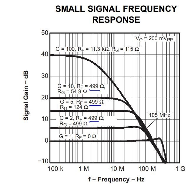
    First of all we need to be sure which model is being used - Here is a generation of Figure 1 in the datasheet, first with the 2005 model and 100ohm load, 

    Then, I noticed they are using 100kohm load, doing that these are closer to the datasheet, 

    Then dropping in the 2020 updated model with 100ohm curves, changes quite a bit - probably a higher input C in the models - that is part of why you use lower R's at low gains as the C introduces another pole in the loop gain, 

    Part of the excel errors is just standard value selection at the lower F, at 1Mhz and gain of 100 you are rolling off at 1MHz. 

  • HI Michael,

    Can you please clarify on below queries,

    1. Can you please confirm on the errors values in my simulation?

    At 42 gain,  error is  2.05%. is it correct?. 

    2. For closed loop gain selection, shall we use any resistors combination?, or as datasheet showing we need to use Rf=499 and change the Rg as per gain requirement?.

    regards,

    Tatarao K

  • Also please us know what will be maximum closed stability gain it will support at 1MHz?, 

  • Can you insert your sim file or tell me what year your model shows. And when you support 1Mhz at what max gain, what do you mean - target error from expected gain?

  • I was looking at one of your datapoints case 1 100Hz and I am suspecting this might not be a simulation

    if the resistor values are perfect you should expect a gain by two terms

    1+Rf/Rg

    then multiplied by the LG/(LG+1) term

    The 1+Rf/Rg term with Rf =499 and Rg = 24 gives 1+Rf/Rg =21.79

    The Loop gain is the Aol/(1+Rf/Rg). The low frequency Aol is 80dB (Figure 12 in datasheet). Then the LG/(LG+1) term is 0.9978

    So the overall gain at 100Hz should be 0.9978*21.79 = 21.74 (or 26.74dB, exactly matching your case 1 dB gain at 100Hz)

    However, neither the original nor the 2011 model updates show the correct Aol curve at 80dB DC with about 20kHz dominant pole. This suggests to me your data is measured? Not simulated, correct? 

  • HI Michael,

    Could you please share the latest model of THS463DDA for simulation. We are planning to do simulation in LT spice.

    regards,.

    Tatarao K

  • The latest models are in the web product folders under simulation tools. 

  • Here is that test file for the Aol response, you can see the 2011 model (which I think is the latest) is not matching the Datasheet low frequency curve at all. You might look at the much more recent OPA810

    and the file in V7 format, 

    Aol curve generation for THS4631 new model.TSC

  • Hello,

    To clarify, the latest model is the 2020 version which can currently be found in the product page or using the following link:

    In regards to the question of choosing your gain setting resistors, there is a tradeoff to both increasing & decreasing the feedback resistor value. Lowering the feedback will result in increased power dissipation from from the device since overall load seen by the output will be reduced. Setting the feedback resistor too high will lower your bandwidth and may have an effect on stability as the resistor interacts with parasitic capacitances. I would recommend starting with the recommended 499 ohm resistor in the datasheet & tuning based off your needs. 

    Best,

    Hasan Babiker

  • Oops, I thought I had the latest model, that 2020 update looks much better on the Aol sim vs the datasheet plot, yes 80dB DC Aol with 200Mhz BW. perfect it looks like, 

    And this file in V7

    Aol curve generation for THS4631 2020 model.TSC

  • HI Michael,

    Thanks for extended support. Could you please clarify below queries.

    1. We have used below Model for simulation, downloaded  from TI website. Is this Model is Latest?.

    2. We did simulation in Tina and captured gain errors for different closed loop gains at 1MHz, please confirm these errors are correct at 1MHz? or not?.

    case 1: Closed loop gain is 21.7, error is 0.46%.

    case 2: Closed loop gain is 36.5, error is 1.49%

    case 3: Closed loop gain is 42.4, error is 2.05%

    case 4: Closed loop gain is 101.7, error is 10.46%

    3. I am using below resistors values for 20 & 10 closed loop gains, is this values are ok to use?.

    For 20 gain, Rf=499R, Rg=26R

    For 10 gain, Rf=499R||470, Rg=26R

    Regards,

    Tatarao K,

    9059058519

  • Hello Tatarao,

    Would you mind posting again using the "Insert/Edit Media" button to post your images? The pictures didn't come through in your latest post.

    Best,

    Hasan Babiker

  • But by way of preview Tatarao, 

    Your gain error at higher gains and 1MHz is just the response rolling off as it should. If you want better flatness through 1MHz and gain of 100, use a faster VFA or a CFA device like the OPA684. 

  • If you want perfect flatness at a gain of 100 through 1MHz, one option is the OPA684 - we did that with closed loop input stage CFA to really extend the gain range on a low power CFA, not FET input of course, but here you go, broadband, 

    and then just over a 10kHz to 1Mhz span, pretty flat, 

    And then the file, in V7

    OPA684 non-inverting gain of 101.TSC

  • HI Michael,

    Thanks for extended support. Could you please clarify below queries.

    1. We have downloaded  Model from below link for simulation, downloaded  from TI website. Is this Model is Latest?.

    Model: SLOM248A.ZIP (4 KB) - TINA-TI Spice Model

    THS4631 data sheet, product information and support | TI.com

    2. We did simulation in Tina and captured gain errors for different closed loop gains at 1MHz, please confirm these errors are correct at 1MHz? or not?.

    case 1: Closed loop gain is 21.7, error is 0.46%.

    case 2: Closed loop gain is 36.5, error is 1.49%

    case 3: Closed loop gain is 42.4, error is 2.05%

    case 4: Closed loop gain is 101.7, error is 10.46%

    I want to use this Part at 40 Closed loop gain, please let me know it will have gain stability at 40 gain for1MHz?.

    3. I am using below resistors values for 20 & 10 closed loop gains, is this values are ok to use?.

    For 20 gain, Rf=499R, Rg=26R

    For 10 gain, Rf=499R||470, Rg=26R

     1385.THS4631_Gain Vs Freq.xlsx

  • Hello Tatarao,

    To answer your questions:

    1) Yes this is the latest version of the THS4631 model.

    2) It is difficult to confirm your sims without knowing your exact configuration, can you provide your TINA circuit for each case? As Michael mentioned at higher gains you may be seeing rolloff in which case you will need a faster amplfier. On the other hand the THS4631 is also a sensitive device that may exhibit peaking and at times needs a feedback capacitor to lower peaking, as indicated on figure 2 of the datasheet. 

    Can you also clarify what your load conditions are in this case?

    3) I don't see a major issue with using these particular values, however you should be wary of the output swing of your device when lowering the feedback resistor in your gain of 10 configuration. Sims are showing output will be limited to around Vs+ - 3.5V in this case.

    Best,

    Hasan Babiker

  • HI Hasan & Michal,

    Queries regarding THS4631DDA,

    1. I am using V+=15V and V - =-5V power rails for THS4631DDA, is this device need heatsink?. what will be the maximum power consumption when device is operating?.

    2. Can you please verify and conform on gain errors?.7103.THS4631_Gain Vs Freq.xlsx

    3. TH4631DDA output swing limiting to 9V, is this ok?

  • Hello,

    To answer your questions:

    1. For improved thermal performance, please use either the DDA or VSSOP package for this device,. Both of these have a PowerPAD available in the package. 
    2. It is difficult to say for sure how closely the results will match between simulation results & measured data due to parasitics that can be introduced in real world situations. However the results should not vary too much if you are getting these values in sim and confirming with results in the datasheet (like the figure you included in your initial post).
    3. With a 100-ohm load you should be able to swing to 10V or at the very least 9.5V. What is the load you are using here?

    Best,

    Hasan Babiker

  • HI hasan,

    Thanks for reply,

    1. i am using THS4631DDA package, hope heatsink is not required, i am right?.

    2. I am doing 2 layer PCB Layout for THS4631DDA, this device placed on TOP Layer and bottom layer is GND.

    may i know purpose of the removing GND plane and POWER plane under THS4631DDA device pins?.

  • Hello,

    1) No a heatsink shouldn't be necessary if you are following the steps under "PowerPAD PCB LAYOUT CONSIDERATIONS" for your layout & the device is being used in a typical fashion.

    2) This is to reduce parasitic capacitance at the input & output pins of the device, which is recommended for many high speed amps. Here is the explanation from the datasheet:

    Best,

    Hasan Babiker

  • HI Hasan,

    Could you please let me know, what is the Voh(min) ?, if VCCB=1.8V for SN74AVC2T245RSWR device.

  • Hello Tatarao,

    I cover high speed amplifier devices, please start a new thread to discuss with an expert on the SN74AVC2T245RSWR.

    Best,

    Hasan Babiker 

  • HI Hasan,

    Regarding THS4631DDA,

    1. I am using 499R for for Gain 20, and 499R parallel with 470R for Gain 10 with 0603 packages, please let me know if any issues with these resistors values & packages.

    2. Power supplies 15V & -5V using as shown below, please let me know if any issues with these unbalanced power supplies in terms of performance degrade offset, CMMR, etc.

  • Hello Tatarao,

    1. Can you clarify what your load is here?

    2. Unbalanced supplies shouldn't have an impact on the performance of the device as long as you are remaining between the input & output limitations. 

    Best,

    Hasan Babiker

  • HI Hasan,

    1. we are not connecting any load, just measuring the output voltage with scope. Scope input impedance will be the load.

    regards,

    tatarao K

  • Hello Tatarao,

    I meant what will be the load in your final application?

    The only issue with using the 470-ohm resistor in parallel is that your output voltage range will be limited because of your output current consumption. See below for the difference in your maximum output voltage with a high-impedance load in both situations:

    Best,

    Hasan Babiker

  • HI Hasan,

    1. For these 499R, 470R and 26R resistors i am using 0603 packages, will this package is fine?, or need to use more then this package?.

    2. or else please suggest me suitable resistors & packages for Gain 20 & Gain10.

  • Hello Tatarao,

    Yes, using the 0603 package should be fine here. Suitable resistor values will vary based off your requirements:

    1. You mentioned your load is the scope, but do you plan on using this device with another load in the future or an ADC possibly? Are you using a 50-ohm or high impedance load for the scope?
    2. What is your required maximum & minimum output voltages? 
    3. Do you have any specific noise requirements?

    Best,

    Hasan Babiker

  • HI Hasan,

    1. I am measuring THS4631DDA output with scope, i did not connect any load separate load at output side.

    2. Output voltages from 1mv to 8.5V

    3. Noise should be as low as minimum, output should be 2% accuracy.

  • also shall i use below resistors for 30Gain and 15gain?,

    for 30 Gain, Rf=2K, Rin=70R,

    for 15Gain, Rf=2K parallel with 1.8K & Rin=70R

  • Thanks Tatarao,

    I think you shouldn't have an issues meeting your requirements for your gain of 10 & 20 configurations. What is the reason for switching to a 2k resistor for the gain of 30 condition? 

    I think you may get better accuracy maintaining a consistent feedback resistor value & varying your gain resistor (RG) to change the gain instead. IT should be noted also, that the tolerances of your resistors here will have an impact on your accuracy.

    Best,

    Hasan Babiker

  • HI Hasan,

    With 20Gian i am getting 8.5V output , to get 11V output planning to use 30Gain. for this i have selected Rf=2K & Rin=70R. to limit the power dissipation i have selected Rf in kilo ohms range.

    and 15Gain, i have selected Rf1= 2K parallel with Rf2=1.8K and Rin =70 ohm.

    please let me know your suggestion on this.

  • HI Hasan,

    If 24.7mA current will passing through R1 499, we need more then 0.287W resistor package, right?.

    0603 package having 0.1W only.

  • Hello Tatarao,

    That is correct you would need a resistor with a rating of at least 304mW. If you are unable to switch to a resistor with a higher power rating, you can increase the resistance of RF & lower RG to meet your gain requirement.

    Best,

    Hasan Babiker

  • HI Hasan,

    Earlier i have selected Rf=499R & Rg=26.1R for 20 Gain, and Rf1=499R parallel with Rf2=470R & Rg=26.1R for 10Gain.

    If we use these resistors power dissipation will be more.

    So i am planning to use higher resistors values, like Rf=1.5K & Rg=75R for 20 Gain, and Rf1=1.5K parallel with Rf2=1.3K & Rg=75R for 10Gain.

    Please let me know if any issues by using these high resistors values?

  • Hello Tatarao,

    If you are unable to increase the power rating of your resistors, I agree increasing your feedback resistors in the kohm range would be the safest choice. I don't forsee any major issues, but as mentioned before this will increase your noise and can have an impact on your bandwidth. I would suggest testing your circuits in SPICE to confirm you are still meeting your bandwidth and noise requirements & if not tuning your feedback resistors further.

    Best,

    Hasan Babiker

  • HI Hasan,

    If i use below resistors, what package would be needed? 0805 or more ?. please suggest

    Rf=499R & Rg=26.1R for 20 Gain, and

    Rf1=499R parallel with Rf2=470R & Rg=26.1R for 10Gain.

  • Hello Tatarao,

    The question is less a matter of the package size but rather the power rating of the resistors you use.

    Best,

    Hasan Babiker

  • HI Hasan,

    I am doing testing for below circuit.

    Using Rf=1K & Rg=51R for Gain 20, and  Rf1=1K parallel with Rf2=1K & Rg=51R for Gain 10.

    For low current(1uA to 100uA) and High current(100uA to 10mA) 1st stage op amp giving expected output voltages(8mV to 0.8V).

    but for Low current(1uA to 100uA) 2nd stage op amp(THS4631DDA) not giving expected output voltages(170mV to 8.7V), we are getting low voltages only. for example instead of 4V, we can see 1.8V only.

    Please let me the reason?.

  • Also please let me know use of Z3=950 in EVB.

  • Hi Tatarao,

    the 950R resistor is used to provide a 1k load to the OPAmp when connecting it to equipement with 50R input impedance :-)

    Kai

  • HI Kai,

    Thanks for reply...

    Please let me know how to calculate this Load resistor value? 

    For below circuit, what would be the Load resistor(RL) value?

  • Hello Tatarao,

    This will depend on a few factors:

    • Whether or not you are trying to drive a capacitive load?
    • What your load resistance will be? Are you using a 50-ohm load here?
    • Desired output voltage.. you don't want RL to be too high as to attenuate your output but also don't want your output current to limit the max output of the device. 

    Best,

    Hasan Babiker

  • HI Hasan,

    1. THS4631DDA output is connecting to DVM(Impedance=10M) & Scope(Impedance=1M) to measure the output voltage.

    while measuring with scope, I can measure the actual output voltage(8.7V) with out RL(RL=0R),

    but while measuring with DVM, i can not get the actual output(8.7V), i can see in the less voltages like 1V or 1.5V only in DVM.

    If RL=2.7K, then only i can measure the actual output voltage with DVM...

    Please let me know  what is the issue?. how to calculate  Load resistor RL for below design?.

  • Hi Tatarao,

    a DVM can show a huge input capacitance destabilizing the THS4631 by too high capacitive output loading. This is often overlooked when connecting a DVM directly to the output of OPAmp without introducing a suited isolation resistor. Usually an isolation resistor of 50...100R is sufficient, but maybe the THS4631 needs a bit more.

    Kai