This thread has been locked.
If you have a related question, please click the "Ask a related question" button in the top right corner. The newly created question will be automatically linked to this question.
Hi all,
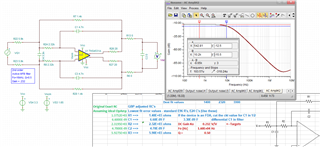
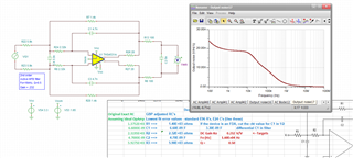
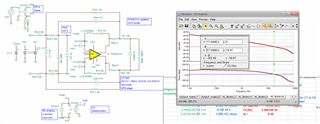
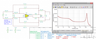
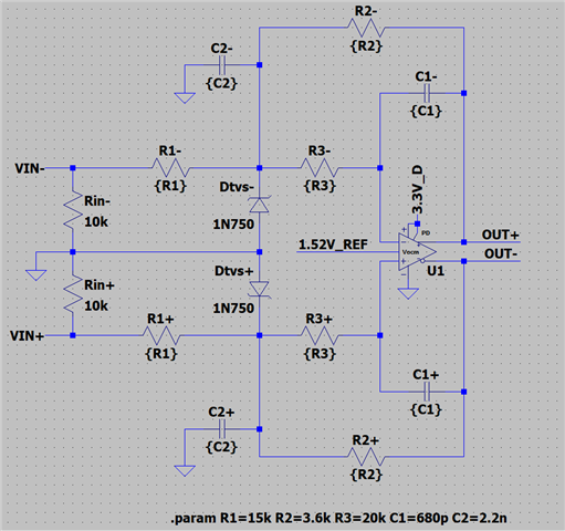
I'm developing an analog conditioning circuit to drive an ADC (0-3V) from an analog input -10/+10V of my system, using THS4531A. Around that part, I designed a MFB filter with DC Gain = -0.232, Fcut = 16kHz and Q = 0.5. It seems to be working without any stability issue in simulation.
I've just read an application note https://www.ti.com/lit/an/slyt336/slyt336.pdf where possible stability issues with FDAs and gain <1 are discussed, and a solution with an input voltage divider is proposed.
Now, I would like to know if my circuit (that doesn't use such an input voltage divider) can experience stability issues. Is there anyone who has experience with this FDA and can help me?
Best regards,
Alessio
Morning Allesio,
It is unfortunate that app note is still out there by Jim Karki, It is completely wrong and misleading, this comes up so often, I devoted an article to the topic,
Not sure you need those 10kohm to ground, the differential MFB shows an input impedance on each side equal to that 1st resistor, if you have an input impedance in mind, can just target that value
Also Allesio, those zeners are adding quite a lot of capacitance in parallel with those C2 elements, not sure you really need those 4.7V zeners
here is an option Allesio,
I adapted an earlier circuit to this so ignore the numbering the schematic (but not the values) the RC numbering is in the table below with the ideal single ended schematic to the lower right
1. Your are getting about 6kohm input Z now on each side, so I just designed for that
2. Those 20ohms inside the loop at the output are optional, we find it helps stability sometimes with that feedback C sitting there on the reactive output stage impedance
3. I collapsed your caps to ground to a single differential C and got rid of the zeners
4. You said 16kHz cutoff - wasn't sure if that was Fo or F-3dB, I used it as Fo and get about 10.2kHz F-3dB
5. If I knew how to insert sim files I would, but not yet,
A quick way to check for low phase margin is to look at the output differential noise broadband - and indeed we do with that sharp spike at 40Mhz, easy to fix, I will work on it a bit,
Let me try and attach the file, also, I would not go further with this without more info on the load - right now I have that as nothing, but if there is something RC wise there I would need to have it for stability improvement work, well I have tried that insert tool and no luck copying the file into that window or top bar that says URL/file
Hello Michael, many thanks for your explanation, I will take a deeper look in a while.
At the output there is a RC stage both for Out+ and Out-, as charge-buck for the subsequent SAR ADC. Both capacitors are connected to ground.
Putting that loading on, seems to have fixed the resonance at higher F. I used a differential 5nF, same as two 10nF to ground.
I had another file already set up for LG phase margin for this kind of circuit, adjusting that to my RC values with 0ohm inside the loop gives 18deg phase margin. If I increase those to 50ohm each for the Riso here, it goes to 34deg phase margin - important to connect the filter feedback C outside those to get the improvement.
Here is this file if you wanted to try it with your RC values, etc. The other tuning point here is that Ctune right across the input pins, that shapes the noise gain up at higher F increasing phase margin.
I was wondering why with 18deg phase margin with those Riso =0ohm I was not seeing a noise spike, I made the classic mistake of looking after the RC filter instead of the output pins - yes, If I look there the circuit nominally low phase margin as shown by the noise spike