- Ask a related questionWhat is a related question?A related question is a question created from another question. When the related question is created, it will be automatically linked to the original question.
Hi,
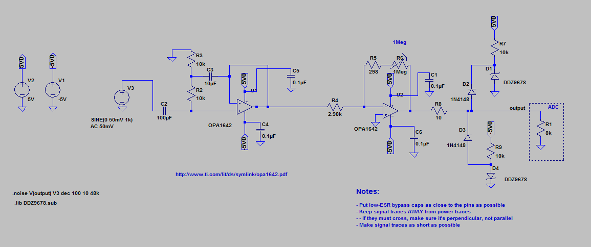
I'm working on a product that requires signal conditioning of an audio signal from a wide variety of sources to under 3 V peak (for the input of an ADC). Technically the full-scale input should be about 1.15 V peak but in order to avoid damaging the ADC it must be kept under 3 V peak. Noise should be kept to the minimum possible.
To accomplish this, I designed this schematic using the OPA1642 audio op amps. The input stage is set up as a unity buffer with a bootstrap for high input resistance. The second stage is set up to provide gain anywhere from 1/10*Vin to 333*Vin. Finally the output is clamped to about +/- 2.5 V to protect the ADC.
The idea is that the user will be able to adjust the gain to maximize the ADC's resolution.
I'm looking for general feedback on the design of the circuit as I've never attempted something like this. It seems to work well in simulations. One problem I've noticed is that the second stage contributes a lot to the noise output in simulations when the pot (R6) is turned up (output~250 nV/root-Hz). Oddly enough, R4 is shown to contribute the most to the noise output in the simulation, where I would have expected R6 to be the noisiest at high values. I'm not sure how to get the range of gain I need with less noise though.
Any help, pointers, criticisms are much appreciated!