This thread has been locked.

If you have a related question, please click the "Ask a related question" button in the top right corner. The newly created question will be automatically linked to this question.

PCM3168A: PCM3168A Grounding Recommendation

Part Number: PCM3168A
Other Parts Discussed in Thread: TIDA-00609

Hello everyone,

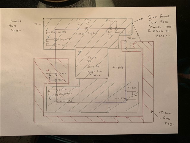
i would be looking for some suggestions regarding AGND/DGND coupling of the PCM. For me, the datasheet-recommendation is not completely clear. "all pins should be connected under the part"?

--> does this mean, i should use only a single GND, both for AGND and DGND? The Reference Design TIDA-00609 uses a similar technique, but it does some kind of inconsequent:

One of the DGNDs is directly connected to AGND (because of part placement i guess), also AGND and GND are connected via some ferrites far outside the part. Also, it seems there is no direct return path for the I2S Digital signals, outside from the "big loop" around the ferrites. there is no direct GND path on the near layers. since the ferrites are ... ferrites, the return current from the digital signals would need to pass some significant inductance and signal quality might suffer.

It seems the design is very suboptimal here.

Now, what would be a better approach? Maybe not to use ferrites, but to use a star-connection of Grounds below the IC? Or is separating the AGND even necessary? the DEM-DAI3168A EVM seems to just connect all grounds directly together.

Thanks alot!

12.1.2 Grounding (AGNDAD1/2, AGNDDA1/2, and DGND1/2) To maximize the dynamic performance of the PCM3168A device, the analog and digital grounds are not connected internally. These pins should have very low impedances to avoid digital noise and signal components feeding back into the analog ground. All ground pins should be connected directly to each other under the part, and the device should be connected to the analog ground of the application, as with acceptable analog layout practices; this layout reduces the potential of noise problems.

  • Care needs to be taken that switching transitions in the digital circuits should not couple into the analog circuits.

    One approach can be as is done in the  EVM and in datasheet. There is a generous single Ground plane here. Local decoupling caps are placed close to their respective pins.Y ou can join the Digital ground pins together with traces and then join with Via to ground Plane. The same can be done with analog ground pins. This forms local zones in the planes where the digital and analog currents circulate.

    -------

    I enclose another approach of 2 Ground planes ,a Digital and an Analog Ground. Local Decoupling Capacitors are placed close to supply and respective grounds. The Analog Ground plane (In Green)includes the power Pad. The Digital Ground Plane joins to the analog Ground Plqne at a single point which we refer to as the Star ground. The Star ground can join to the Analog Ground of the Board.  

  • pins

    Hey Sanjay, thanks for your great effort! 

    Actually, it seems to be kind of similar what i had in mind. If it is possible, do you want to take a quick look at my design? Per Mail would be ideal.

    --> I do have an Overlap of ~3cm² of AGND and DGND with Core inbetween, but like this, I2S Lanes and 3V3 are shielded from any analog path.

    Anyway, i think the topic is a bit clearer now :)

    Best regards,

    Lukas