This thread has been locked.

If you have a related question, please click the "Ask a related question" button in the top right corner. The newly created question will be automatically linked to this question.

OPA1641-Q1: On the input voltage buffer of microphone audio acquisition

Part Number: OPA1641-Q1
Other Parts Discussed in Thread: INA1650, JFE150, INA1620

ALL HI!

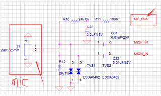
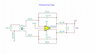
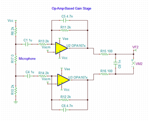
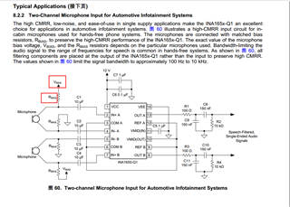
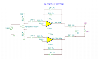
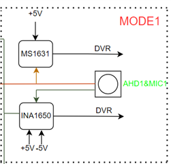
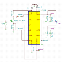
As shown in the figure below. The left J1 is the position of the external microphone. If I can't determine the mic_ The size of bias and the input voltage range of audio ADC used are 0 ~ 3.3V. How to put micp_ In and MICn_ In connected ADC input, how to design the buffer. thank you!

  • MIC_ Bias may be very large, such as 12V

  • Hi Sheng,

    There are many different ways a buffer can be implemented, depending on the details of the design.  Here are some more details we would need to get an answer to before we can move forward:

    - What is the application?  Is this a voice-only microphone?  This will determine how critical noise performance is; many automotive customers use INA1650 for voice microphone buffering because it offers an easy, integrated high input impedance solution and should be considered.
    - What is the ADC part number?  If you don't know the specific ADC yet, do you know if the input to the ADC is differential or single-ended?
    - What is the voltage amplitude is coming from the microphone?  Is there a need for attenuation into the 3.3 V ADC?  Best case would be that you can send the microphone part number so we can understand how the biasing works internally (i.e. JFET, bipolar, transformer, etc)

    Once we get some of these details we can narrow down the design.

    Best Regards,
    Mike

  • thank you! Michael!

    As shown in Figure 1 below, it is the introduction and block diagram of ADC, and the input is differential input. The upper limit of input voltage is - 0.3V ~ 3.6V.

    As shown in Figure 2, it is the driver's pager on the bus. The circuit is very simple. A and B are the leads at both ends of MIC. SW is a button switch. You can talk with each other when you press and pop up once, and close when you press and pop up again. If this MIC is connected to ADC, how to design the bias voltage? How to add a buffer? Can ina1650 be used in this application? How do I use it?

                             Figure 1

                       Figure 2

  • Hi Sheng,

    Without any further info., I'll assume that this microphone is a dynamic mic., which are very common for vocal mics. Since dynamic mics. typically use a transformer in the output stage, they don't require any DC biasing, so the interface is relatively simple.   Here's an example of an easy ways to implement a dynamic mic. interface to an ADC.  The first will be to use two separate amplifiers (or a single dual amplifier IC) to tap the positive and negative ends of the microphone transformer output.  See the schematic below:

    In this case, the mic. output terminated with 2kOhm resistors to virtual GND, which is represented by Vocm voltage.  The Vocm voltage will offset the output voltage to mid-scale (1.65 V).  The feedback capacitors are used to limit the bandwidth to the necessary vocal frequency range (f3dB = 16 kHz), and the output resistors (100 Ohm) along with the differential cap. are used to provide a "charge bucket" to the ADC input.

    A similar circuit can be used with a fully-differential amplifier (FDA):

    The FDA will have the advantage of the differential noise being lower as a result of it being a single input, versus two different inputs (i.e. OPA) where the noises are uncorrelated noise sources and will RSS together.  Also, the overall current tends to be lower for the same level of noise performance.  

    Your first circuit shows DC bias for the microphone; this could imply that it is an active FET output, in which case, the original circuit I showed would also need DC-blocking caps.  This is many times the case for electret-type microphones.  See the circuit below.

    The primary problem with the circuits above is the common mode rejection is very much dependent on the matching of the input resistors.  If 1% resistors are used, the CMRR can be as low as 40 dB.  This means any common noise will turn into differential noise in the amplifier stage, and potentially corrupt the signal.  This may be OK for basic applications, which sounds like it is the case for your microphone.

    The INA1650 is used for cases where there is long cabling between the microphone location and the ADC and very high common mode rejection is needed (i.e. > 80 dB).  The INA1650 provides a high-input impedance buffer, where the termination resistors are tightly matched.  This means that any low impedance mismatches are minimized since the overall impedance of the circuit is higher.  I don't think this is the case, so, unless you let me know otherwise, I'll skip that one.

    Lastly, the op-amp based circuits above uses an inverting gain stage, which suffers worse noise-gain than the non-inverting gain case.  However the non-inverting gain case tends to need more components.  If very low noise is desired, I can also propose a non-inverting solution, but the noise performance would be similar to the FDA case, and also add additional components.

    I am attaching the simulation I used below.  Please let me know if this helps address your design.

    Best Regards,
    Mike

    OPA1637_mic_input_Jan_2022.TSC

  • Thank you!Mike!

    The explanations were very detailed. I need to read it carefully.As shown in the figure below. Vbias and rbias are the specifications of the microphone I use, and the specific values are given. Not by calculation?

  • Hi Sheng,

    The biasing is specific to the the microphone.  If it is not a dynamic mic., and instead has some sort of capsule, like a condenser or electret mic., then it likely has a FET or possibly BJT output stage. The manufacturer of the microphone module should give guidance as to what those resistor values and bias voltages should be.  If you are saying the bias resistors should be 2.2k, you could understand it referring to an example would be like below, using our JFE150 JFET:

    If it is the case like above, you can use either op. amps (like above) or INA1650, connected as you have shown.  INA1650 will offer high input impedance, so, the CMRR will be good.  However, in the case above, the impedance of the JFET stage is not truly matched because the capacitances of the JFET are different, since the VGS voltage and VGD voltages are different.  So I don't believe the INA1650 would make sense in that case.  However it will be difficult to know unless you can send the microphone data sheet.

    Regards,
    Mike

  • Thank you!Mike!

    As shown in the figure below. Ahd & mic1 is a megapixel analog camera with microphone, and the audio signal amplitude is 1vpp. At present, we want to use an audio buffer (such as ina1650) to transmit to DVR equipment through wire. If an operational amplifier is used to build this audio buffer circuit, how to design this circuit?

  • Hi Sheng,

    You can build a basic audio receiver similar to the circuits I have shown above with discrete OPAs, no problem. However, you will not achieve good CMRR performance unless you use resistors that are tightly matched.  CMRR performance will determine the circuit's ability to reject common-mode noise.  If the CMRR is low, then any ground noise or common-mode coupling will turn into differential noise, effectively defeating the purpose of a differential signal.  The CMRR, though, is strongly dependent on  see below for a summary:

    INA1650 features resistors with excellent matching, which is why the CMRR is so high.  In order to get this kind of matching you would need matched resistors on the order of 0.01%, which can be expensive.

    So, while you can easily build an audio receiver with discrete parts, the resistors themselves are key to the design. Another device with excellent resistor matching is INA1620; this is generally intended for headphone driving, though.

    INA1650 can be easily configured to have differential in, differential out, you only need to use one channel on the positive side and one on the negative side, and shift the REF pins by the necessary common mode voltage (i.e. 1.65 V).  See below:

    Let me know if this helps.

    Regards,
    Mike

  • Thank you!Mike!Thank you very much for your help!