This thread has been locked.

If you have a related question, please click the "Ask a related question" button in the top right corner. The newly created question will be automatically linked to this question.

PCM1808-Q1: Vcc supply timing

Part Number: PCM1808-Q1
Other Parts Discussed in Thread: PCM1808

Hi team,

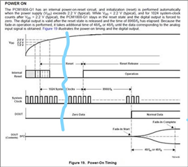
Is it OK to apply 5V to Vcc after Vdd powered up?

In my case, There is a case that Vdd applied first and then Vcc applied at the timing below in blue line. 

Does the device start up correctly? Is there any concern?

regards,

  • Hi,

    the PCM1808 doesn't have any power sequencing requirements. the blocks that Vdd and Vcc power are functionally separate form one another.

    Regards,
    Arthur

  • Hi Arthur,

    Even if Vcc is not applied, the device can receive system clock and then release reset in correct timing?

    What kind of function are affected by loss of Vcc?

    regards,

  • Hi Shinji,

    I would suspect that yes the reset would release. if Vcc needed to be present for this to happen I suspect is would be included in the timing diagram

    But if you don't apply Vcc you wont have any Vref, and then I would expect the ADC to be spitting out garbage data - if it gave any data at all. (because the ADC is referencing the input signal to Vref.

    If you where considering not supplying Vcc to the chip I would strongly recommend that you dont do that ;)

    Regards,

    Arthur

  • Hi Arthur,

    Thank you for the clarification.

    I have just concerned the Vcc timing affect the device power on reset timing or not. 

    I understand Vcc has no impact on device power up. Vcc just required to perform AD conversion. 

    regards,