This thread has been locked.

If you have a related question, please click the "Ask a related question" button in the top right corner. The newly created question will be automatically linked to this question.

PCM1864: noisy output

Part Number: PCM1864

Hello,

We are attempting to use the PCM1864 in our amplifier, however we are getting a lot of white noise and distortion coming out on the speakers when we are either providing an audio signal or nothing, and we have narrowed it down to being a problem with the ADCs.

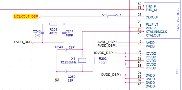
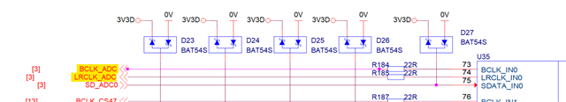
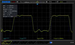
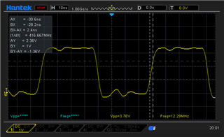
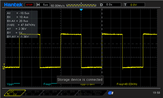
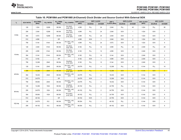
There are 4 PCM1864s, each handling 2 pairs of stereo inputs, they are all in slave mode with the clocks (SCK, BCK and LRCK) being provided by a DSP, an ADAU1467 from Analog Devices, and the DSP is connected to a 12.288MHz crystal. We communicate to the ADCs by I2C and use that to configure the setup of the ADCs. As for the configuration of the ADCs, as mentioned before they are in slave mode and we configure the clocks to follow row 12 of table 10 on page 41 from the datasheet, see the highlighted below:

We also configure the mapping of the inputs to match our hardware setup, the Serial Audio Interface Format to be TDM, 4 channel TDM transmission data and the TDM offset to 1 BCK (same as I2S), all other register configurations are left as their default.

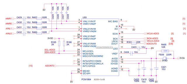
We have tested the system beyond the ADCs by having the DSP generate a test chime and there is no noise or distortion on the chime, so we know that the issue is to do with the ADCs, either how we are configuring the registers or with the hardware design. Our design for the inputs to the ADCs is similar to what is shown in your datasheet, only a slightly variation in resistor and capacitor values, however we have tried changing those values to match the datasheet, but that didn't have any effect on the audio quality, so we don't think the problem is with the inputs to the ADCs. Here is a picture of our schematic for one of the ADCs:

We would appreciate any help or pointers to get us to a solution for this problem.

Thank you

  • Are all 4 devices on the same I2S Bus?

    Are you choosing 16 bit data?  4devices*4 channels*16=256. Therefore BCK=256*fS . Is the BCK 12.244MHZ?

    You should check the Input waveform on the Input Pins of the chip. It should be biased on a 1.65v DC.

    Can you send me the I2C Settings relating to each of the 4 chips

  • No, ADCs 0 and 1 share one bus, and 2 and 3 share another.

    The PCM word length selection in register 11? No, we are selecting 24-bit data, for both the receive PCM word length and the stereo PCM word length.
    But based on what you said and given our setup, should we be choosing 32-bit data? (2 devices * 4 channels * 32 = 256)

    The clock signal on the BCK pin is 12.288MHz.
    Yes, the input signals have a 1.65V bias.

    Sure, here is the clock config that is sent to all the ADCs

    static const uint8_t TiAdcPLL[] __RDONLY = {
        0, 1,	0xFE,   // reset registers
        0, 1,	0x00,   // set to page 0
      113, 1,	0x1F,   // mute all channels
      // fs = 256 PLL_RATIO = 2048 (?)
      // SCK_FREQ = 12.288
      // PLL_FREQ = 98.304 (P = 4, R = 2, J = 16, D = 0)
      // DSP1_CLK = 24.576, DSP1_SRC = PLL, DSP1_DIV = 4
      // DSP2_CLK = 12.288, DSP2_SRC = SCK, DSP2_DIV = 1
      // ADC_CLK  = 6.144,  ADC_SRC  = SCK, ADC_DIV  = 2
    	32, 4,	0x42, // SCK selected, slave mode, ADC clock = SCK, DSP2 clock = SCK, DSP1 clock = PLL, disable auto clock detect
    	        0x03, // DSP1 clock div = 1/4
    	        0x00, // DSP2 clock div = 1
    	        0x01, // ADC clock div = 1/2
    	37, 9,	0x07, // PLL SCK clock output div = 1/8
    	        0x00, // SCK-BCK div = 1
    	        0xFF, // BCK-LRCK div = 1/256
    	        0x01, // PLL enabled
    	        0x03, // PLL P div = 1/4
    	        0x01, // PLL R multi = 2
    	        0x10, // PLL J = 16
    	        0x00, // PLL D (LSB) = 0
    	        0x00, // PLL D (MSB) = 0
    	 0, 0
    };

    Here is other setup config that's also sent to all the ADCs:

    static const uint8_t TiAdcSetup[] __RDONLY = {
         6, 7, 	0x41, // ADC1L channel select: VINL1 (non-inverted)
                0x41, // ADC1R channel select: VINR1 (non-inverted)
                0x42, // ADC2L channel select: VINL2 (non-inverted)
                0x42, // ADC2R channel select: VINR2 (non-inverted)
                0x00, // no selected input channel for secondary ADC
    		    0x03, // rx PCM 24bit word len, LRCK duty cycle = 50%, stereo PCM 24bit word len, SAIF = TDMDSP
    		    0x01, // 4ch TDM
    	16, 6,  0x00, // GPIO1 = non-inverted GPIO, GPIO0 = non-inverted GPIO
    	        0x00, // GPIO3 = non-inverted GPIO, GPIO2 = non-inverted GPIO
    	        0x44, // GPIO1 = output, GPIO0 = output
    	        0x44, // GPIO3 = output, GPIO2 = output
    	        0x00, // clear GPIO status register
    	        0x00, // pull down GPIO3, 2, 1, and 0
    	 1, 5,  0x00, // Ch1L PGA = 0dB
    	        0x00, // Ch1R PGA = 0dB
    	        0x00, // Ch2L PGA = 0db
    	        0x00, // Ch2R PGA = 0db
    	        0x80, // enable PGA smooth change, independent control, disable clip det, attenuation lim = -3dB, clipping suppression after 80 times, disable auto clip suppression
        25, 1,  0x00, // set everything to auto-gain
     	 0, 0
    };

    Here is a TDM offset config sent to ADCs 0 and 2:

    static const uint8_t    TiAdcOffset0[] __RDONLY = {
        13, 2,  0x01, // Tx TDM offset of 1 BCK (same as I2S)
                0x00, // Rx TDM offset of 0 (default)
         0, 0
    };

    And then here is the TDM offset config sent to ADCs 1 and 3:

    static const uint8_t    TiAdcOffset1[] __RDONLY = {
        13, 2,  0x81, // Tx TDM offset of 129 BCK
                0x00, // Rx TDM offset of 0 (default)
         0, 0
    };

  • I would suggest to begin with 1 device alone to see audio performance. You could try slave PLL Mode by just giving BCLK and LRCK  . 48K and 12.288Mhz should work and remove the crystal. Page 77 and 78 describe this mode and settings needed.

    With 1 chip and 2 inputs you can then see if the noise situation is better and then proceed ahead

  • We tried removing the other ADCs, so there is only one connected to a bus, as well as disconnecting the SCKI input to that remaining ADC, so it's only being given BCK and LRCK.

    And it is still being put into slave PLL mode, as shown in my previous reply with the configurations. However we can't remove the 12.288MHz crystal, as it is providing the clock for the DSP chip and isn't directly connected to the ADCs.

    It resulted in us getting nothing out of the one ADC at all, no noise or audio.

    As for the settings described on page 77 and 78 you referred to, as far as I can tell, we are following those settings, the only minor differences are to do with the mic bias and VDD, DVDD, IOVDD and LDO setup, however one of our hardware engineers found these in the datasheet:

    Which suggest that we don't need the mic bias connected and that our hardware setup for the AVDD, DVDD, IOVDD and LDO should be okay.

  • Are you using the Crystal pins to couple a Clock to a DSP?

  • I'm not sure what you mean? In the ADC schematic in my initial post, you can see that we have left the ADCs crystal pins either disconnected or tied to ground.

    But below are the schematics for the clock inputs for the DSP and the signals (which I've highlighted) which are then connected to the SCK, BCK and LRCK clock inputs of ADCs:

  • I was under the impression that you had the crystal connected on the ADC Chip.

    One small comment. Can you please remove D27 just as a test?

    Also do you lose output  when you do the Test with 1 IC and disconnect SCKI from the Chip?

    What happens when you have 1 chip and SCKI connected also? How is the noise then?

  • We tried removing D27, no change to the noise and distortion.

    Yes, when we only have 1 ADC with SCKI disconnected, we lost output from the ADC completely.

    Also no change to the noise and distortion when there is 1 ADC with SCKI connected.

  • Are the Timings that are generated from the DSP Clean?

  • Yeah, they look clean to us.

    This is the SCKI signal:

    This is the BCK signal:

    And this is the LRCK signal:

  • shall reply in a short while

  • I assume that now you have 1 ADC only on your board. Is that correct?

    Is your amplifier driven by the TDM Data that is made by the ADC?

    Does the noise reduce if you ground the 4 inputs of the ADCs.? This can be done by grounding the input side of the 4coupling capacitors to the ADC.

    Also, Have you tested the amplifier standalone to check if it has no noise?

    i
  • Correct, the board only has 1 ADC currently.

    Correct, in the ADC register config settings I send earlier, the ADC should be outputting TDM data.

    As shown in my initial post with the ADC schematic, you can see that we have always had capacitors between the ADC inputs and ground.

    Yes, as I spoken about in my initial post, we have tested the rest of the amplifier from the DSP onwards by having the DSP generate a test chime and there is no noise on the output with that test chime, but as soon as we use the ADC, the noise and distortion appears. Which is why we believe the issue is with the ADCs, either their register configuration or hardware layout.

  • Is your Amplifier an I2S Input amp? When you make a chime does the DSP make an I2S input to this amp?

    I actually was wanting that you ground the input end of the 4 coupling capacitors. This would bring the input pins at  AC Ground.I wanted to check if you heard the hiss in this case also.

    The analog input signals can be removed for this test.

  • Well, yes, but to expand on that, our amp is effectively split into 4 parts:

    1. ADCs at the inputs, which output I2S data that then goes to...
    2. The DSP, which also outputs I2S data that then goes to...
    3. DACs which then outputs an analogue signal that is sent to...
    4. the amplifier modules we use (ICEpower80AM2)

    So are the amplifier modules (the ICEpower80AM2) we're using I2S? no, but the steps before that are, the ADCs, DSP and DACs. Therefore when the DSP makes the chime, it is outputting an I2S signal going to the DACs. 

    As for the grounding of the inputs, that didn't make a difference. With no audio signal on the inputs, but instead shorted to ground, there was still the white noise on the outputs.

  • ok

    Can you please  place a Oscilloscope on DOUT pin of the ADC with audio  input signals ground, Do you see any digital activity on this pin?

  • There is activity.

    Since we hear the audio we put on the input, we would expect that. It is just the audio is extremely distorted and when no audio is being inputted there is still a lot of noise on the output.

  • Shall reply Nov 28

  • At this moment is there only 1 ADC and DSP on the Board? If poor layout is the cause then its best to turn off all other Chips and DC Supplies and Operate chip with a Bench Supply.

    Also is there a 22 ohm resistor in series with BCLK?

    You could also write 0x00 TO PAGE 0 Register 6 to see if the noise with no signal goes away.

    https://www.ti.com/lit/ug/tidud75/tidud75.pdf?ts=1669674308858&ref_url=https%253A%252F%252Fwww.ti.com%252Ftool%252FTIDA-01470

    I am also enclosing a TI Design for PCM 1864 Based system . You could use the exact same setup to see if you observe any issue on your board.

    This might indicate to a layout fault