Other Parts Discussed in Thread: PCM1801
As the description states, I have this chip designed in, but I am not getting any signs of life from it on pin 12.
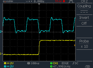
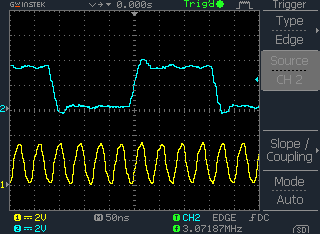
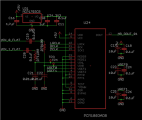
My clock signals as ~3v3 in amplitude, and are being driven by a USB <-> I2S Interface device. I have this device working without issue in other applications, and I also have it working properly with a PCM510xA device, audio sounds good from that device so I think clocks are all looking good. 48Khz, 3.0718Mhz, 24.5749Mhz
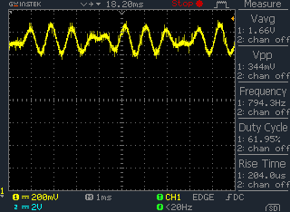
I have confirmed I can get signal (500hz sine wave) into the C19 and C20.
I believe I have everything wired up correctly for the I2S format, but even if that was wrong, I am not getting any data at all from this device on multiple boards.
The only things I have found tonight on the forums that might be a issue is
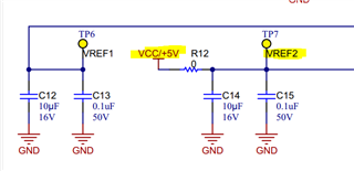
1) the VREF1 (Net)/VREF2(chip) is not tied directly to the 5V as suggested here
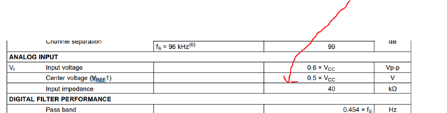
2) The Pins 7 & 17 are driven by 3.3Vdc, where the datasheet is vague with only stating "TTL", is that 3v3 TTL or 5V0 TTL? The specs say 2V should be sufficient, but posts here suggest otherwise. Would this be enough to cause the ~PDWN to treat this as a low and put the device into power down mode?
Is there something else fundamental that I am missing that would cause these devices to not power up / output data