Hello TI team,
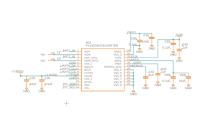
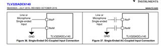
I'm working with TLV320ADC6140 with 2 single ended electret mic lines.
ADC is used in slave 1/2 channel 48kHz 32bit
Im not getting any data on the scope. I noticed that the AREG and MICBias has no voltage.
DREG is at 1.45v, Supplying 3.3V to analog and 1.8V to digital IO
IRQ pin is high but I believe I disabled that. I do measure 48.035KHz on analyzer. Would that put create bus error?
sl_sleeptimer_delay_millisecond(5);
  ADC_Write(I2C0,0x01,0b00000001); // Reset registers
  sl_sleeptimer_delay_millisecond(10);
  ADC_Write(I2C0,0x02,0b10001001); // Sleep Reg - Internal 1.8V Areg, 10ms, not sleep
  sl_sleeptimer_delay_millisecond(10);
  ADC_Write(I2C0,0x07,0b01110000); // ASI I2S 32bit Auto CLK
  sl_sleeptimer_delay_millisecond(10);
  ADC_Write(I2C0,0x08,0b00000000); //
  ADC_Write(I2C0,0x09,0b00100000); // 1 Disable Error detection

  ADC_Write(I2C0,0xA, 0b00010000); // Mixing No mix, -6dB, No inversion
  ADC_Write(I2C0,0xB, 0b00000000); // Slot 0 ch1
  ADC_Write(I2C0,0xC, 0b00000000); // Slot 0 ch2
  ADC_Write(I2C0,0xD, 0b00000000); // Slot 0 ch3

  ADC_Write(I2C0,0x13,0b00000111); // Slave automatic PLL
  //ADC_Write(I2C0,0x14,0b10001000); // not used in slave mode
  //ADC_Write(I2C0,0x15,0b10000010); // Read Only but 44.1-48 1:32 ratio BLCK FSYNC
  //ADC_Write(I2C0,0x16,0b00001000); // CLK_SRC when in Master

  ADC_Write(I2C0,0x21,0b00100101); // GPIO setup Interrupt
  ADC_Write(I2C0,0x22,0b00000001); // IN2M_GPO1 disabled act low
 // ADC_Write(I2C0,0x29,0b10000000); // Interrupt GPIO1 as GPO
  ADC_Write(I2C0,0x2B,0b00000000); //

  ADC_Write(I2C0,0x32,0b00000000); // INT ACtive high
  ADC_Write(I2C0,0x33,0b00000000); // Masking interrupt
  ADC_Write(I2C0,0x36,0b11100000); // Interupt config ASI PLL MIX Int
  ADC_Write(I2C0,0x3A,0b01100000); // Common Mode avdd peak
  ADC_Write(I2C0,0x3B,0b00000001); // IN2M Bias 2.5v
  //ch1
  ADC_Write(I2C0,0x3C,0b00100000); // CH1 setup Mic Single AC 2.5k DREoff
  ADC_Write(I2C0,0x3D,100); // CH1 Gain
  ADC_Write(I2C0,0x3E,100); // CH1 volume
  ADC_Write(I2C0,0x3F,0b10000000); // CH1 gain calibration
  //ch2
  ADC_Write(I2C0,0x41,0b00100000); // CH2 setup Mic Single DC 2.5k DREoff
  ADC_Write(I2C0,0x42,100); // CH2 Gain
  ADC_Write(I2C0,0x43,100); // CH2 volume
  ADC_Write(I2C0,0x44,0b00010000); // CH2 gain calibration

  ADC_Write(I2C0,0x6B,0b00100001); // DSP DRE HPF
  ADC_Write(I2C0,0x6C,0b00000000); // DSP clipping, volume control,
  //ADC_Write(I2C0,0x6D,0b00100000); // DRE config Dynamic Range Enhance
  //ADC_Write(I2C0,0x70,0b00100000); // AGC config Automatic Gain Control

  ADC_Write(I2C0,0x73,0b01000000); // Channel enabling input, EN1 En2

  ADC_Write(I2C0,0x74,0b01000000); // Channel enabling output, En1 En2

  ADC_Write(I2C0,0x75,0b11110000); // Power controls
  //ADC_Write(I2C0,0x76,0b11000000); // ADC power up
  //ADC_Write(I2C0,0x77,0b11100000); // Active mode