TLV320DAC3203: Loopback control register setting

Part Number: TLV320DAC3203
Other Parts Discussed in Thread: MSP430FR2633

Tool/software:

Hi dear people,

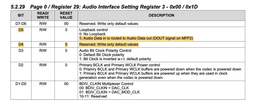
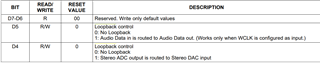
I encounter a discrepancy between the recommended setting for Page 0 / Register 29: Audio Interface Setting Register 3 - 0x00 / 0x1D and that what the information about this register says.

On the script for Digital Mic loopback inside the GUI of the EVAL board, the value written to this register is 0x10, which would be 00010000 and would write D4 = 1

But D4 is reserved and should alwys be 0. Instead, is by D5 = 1: Audio Data in is routed to Audio Data out (DOUT signal on MFP2)

So the value written to 0x1D should instead be 0x20 (00100000)?

Strange enough, the script works fine on the EVAL, although there no phisical connection exists between the DIN and DOUT pins (a hardware-solution suggested here: https://e2e.ti.com/support/audio-group/audio/f/audio-forum/558353/tlv320dac3203-digital-microphone-pdm-to-headphone-output)

On my board, however, I get no audio from the mics on my HP outputs.

Am I (again) misreading the data?

Best regards,

Gustavo

  • Update after checking with the EVAL:
    Changing "0x1D = 0x10" to "0x1D = 0x20" does not work and the result is only noise at the output.

    So, 00010000,  D4 = 1 is correct and the table 5.2.29 not?

    Best  regards,

    Gustavo

  • Hello Gustavo,

    Bit 4 is reserved in register 0x1D and the loopback bit is B5 as you correctly pointed out. So if you want to enable the loopback in reg 0x1D, it should be 0010 ( i.e., 0010 0000 or simply 0x20)

    When you write ONE on B5 of this register , Audio Data  is routed to DOUT signal on MFP2, do you see it at the pin?

    Before we dig  more into it, can you share the schematic of your board,  as well as exact values of your I2S , Micbias and etc..

    Regards,

    Arash

  • Hi Arash,

    thank you for replying so quickly.

    No, I do not see any data on DOUT. Also not on the EVAL.

    I again changed the setting on the EVAL to 0x20, but then audio stopts working.

    But, here I begin to ask myself, if we are talking about the same thing:

    I am working with single bit PDM output mics from Knowles (spk0641ht4h-1).

    So, no I2S, but PDM.

    When Ti speaks about "digital microphones" I assume, is talking about PDM and the example "Digital Mic loopback" inside the GUI refers to the same. There, the script writes a ONE to bit 4 and the script works.

    Again: writing ONE to bit 5 does not work.

    Now, the mic connectors on the EVAL have the DIGMIC_PWR pins feeded with the voltage one can choose by W2 being 3.3 V or 1.8 V. The MICBIAS voltage is not used there for those mic connectors, but for a possibility to have a HP mic on the headphone jack.

    I, however, want to use MICBIAS to be the VCC for my mics. For this I am using the following setting:

    # Set MICBIAS = LDOIN = Power Supply (00111000)
    w 30 33 38
    #  Power on MICBIAS. Voltage source = LDOIN/HPVDD (01111000)
    w 30 33 78

    On the EVAL, since IOVDD is 3.3 V, I get MICBIAS = 3.3 V
    On my board, IOVDD is 2 V and then I get MICBIAS = 2 V This is fine.

    Further, to make problems bigger, I write those commands into the device, using a MSP430FR2633, which, when I use an emulator to communicate with it, receives 3.3 V. Therefore, the DAC3203 gets during this procedure 3.3 V on IOVDD and on LDOIN too.

    This should not be a problem. I tested on the EVAL by setting DIGMIC_PWR to 1.8 V. I get there then DIGMIC_CLK and DIGMIC_DATA between 0 and 1.8 V.

    However, on my board is chaos:

    - MICBIAS is 2 V during programming, while it should be 3.3 V (remember, LDOIN is by programming 3.3 V)
    - The device is heating a lot (75°C and going higher)
    - DIGMIC_CLK is between 0 an 3.3 V, while DIGMIC_DATA is between 0 and 2 V

    So I figure I burned out the 11th device already, without achieving anything more than white hairs  on my head (if I have any left).

    The question is why, since the hardware was ok, till todas, when I started changing the script.
    Here is the complete script. Maybe you discover something causing this.

    # ----- Select Page 0
    w 30 00 00
    # ----- Initialize the device through software reset
    w 30 01 01
    # ----- Select Page 0
    w 30 00 00
    # ----- Clock Setting Register 1, Multiplexers - 0x00 / 0x04 Value= 00: PLL Clock is MCLK
    w 30 04 00
    # ----- DO NOT USE PLL
    w 30 05 12
    # ----- Clock Setting Register 6, NDAC Values - 0x00 / 0x0B
    # ----- NDAC = 1, divider powered on
    w 30 0b 81
    # ----- Clock Setting Register 7, MDAC Values - 0x00 / 0x0C
    # ----- MDAC = 2, divider powered on
    w 30 0c 82
    # ----- DOSR = 128
    w 30 0d 00
    w 30 0e 80
    #  ----- NADC=2
    w 30 12 82
    # MADC=2
    w 30 13 82
    # AOSR = 64
    w 30 14 40
    ###############################################
    # ----- Digital Loopback (Page 0 / Register 29: Audio Interface Setting Register 3 - 0x00 / 0x1D = 00100000)
    ###############################################

    w 30 1D 10

    # -----  THIS DOES NOT WORK.
    # ----- D5 Loopback control = 1: Audio Data in is routed to Audio Data out (DOUT signal on MFP2)
    # ----- w30 1D 20

    ###############################################
    # ----- Configure Power Supplies
    ###############################################
    # ----- Select Page 1
    w 30 00 01
    # ----- Disable internal crude AVdd in presence of external AVdd supply
    # ----- or before powering up internal AVdd LDO
    # ----- Disable weak AVDD in presence of external AVDD supply
    w 30 01 08
    # ----- Power up AVDD LDO (00001001) D3 = 1 Analog Blocks Disabled !!!
    w 30 02 09
    # ----- Enable Master Analog Power Control (0000001) D3 = 0 Analog Blocks Enabled !!!
    w 30 02 01
    # ----- Analog Input Quick Charging Configuration Register - 0x01 / 0x47
    # ----- (Page 1 / Register 71: Analog Input Quick Charging Configuration Register - 0x01 / 0x47) (00110010)
    # ----- D5-D0 = 110010: : Analog inputs power up time is 6.4 ms
    w 30 47 32
    # ----- Set the REF charging time to 40ms (Page 1 / Register 123: Reference Power-up Configuration Register - 0x01 / 0x7B)
    # ----- D2-D0 = 001: Reference will power up in 40ms when analog blocks are powered up
    # ----- w 30 7b 01
    # ----- D2-D0 = 101: Force power up of reference. Power up time will be 40ms
    w 30 7b 05

    ###############################################
    # ----- MICBIAS (Page 1 / Register 51: MICBIAS Configuration Register - 0x01 / 0x33)
    ###############################################
    # ----- Set MICBIAS = AVDD = Power Supply (00000000)
    # ----- D6 = 0: MICBIAS powered down
    # ----- D5-D4 = 00: MICBIAS = 1.04V (CM=0.75V) or MICBIAS = 1.25V(CM=0.9V)
    ###############################################
    # ----- First I used this D3 = 0: MICBIAS voltage is generated from AVDD
    ###############################################
    # ----- w 30 33 00
    # ----- Power on MICBIAS (01100000)
    # ----- D6 = 1: MICBIAS powered up
    # ----- D5-D4 = 10: MICBIAS = 2.075V(CM=0.75V) or MICBIAS = 2.5V(CM=0.9V)
    # ----- w 30 33 60

    ###############################################
    # ----- But now I am using this
    ###############################################

    # ----- Set MICBIAS = LDOIN = Power Supply (00111000)
    # ----- D6 = 0: MICBIAS powered down
    # ----- D5-D4 = 11: MICBIAS is switch to power supply
    ###############################################
    # ----- Using this D3 = 1: MICBIAS voltage is generated from LDOIN
    ###############################################
    w 30 33 38
    #  ----- Power on MICBIAS. Voltage source = LDOIN/HPVDD (01111000)
    # ----- D5-D4 = 11: MICBIAS is switch to power supply
    # ----- D3 = 1: MICBIAS voltage is generated from LDOIN
    w 30 33 78

    ###############################################
    ###############################################
    # ----- Configure ADC Channel
    ###############################################
    # ----- Select Page 0
    w 30 00 00
    # ----- Configure MISO as clock output for DIGMIC
    w 30 37 0E
    # ----- LADC and RADC enabled for DIGMIC
    # ----- Route SCLK as DIGMIC_DATA
    w 30 51 10
    # ----- Power up LADC/RADC
    w 30 51 DC
    # ----- Unmute LADC/RADC
    w 30 52 00
    # ----- disable Din and Dout
    w 30 36 00
    w 30 35 10
    ###############################################
    # ----- Configure DAC Channel with Soft Stepping
    ###############################################
    # ----- Select Page 1
    w 30 00 01
    # ----- Set HP power up time for NO POP
    w 30 14 25
    # ----- Left DAC reconstruction filter +ve terminal to HPL
    # ----- Bit 3 = 1: Left Channel DAC reconstruction filter's positive terminal is routed to HPL
    w 30 0c 08
    # ----- Left DAC reconstruction filter -ve terminal to HPR
    # ----- Bit 4 = 1: Left Channel DAC reconstruction filter's negative terminal is routed to HPR
    w 30 0d 10
    # ----- Unmute HPL/HPR driver, 0dB Gain
    # ----- Page 1 / Register 16: HPL Driver Gain Setting Register
    # ----- HPL driver gain is 0dB
    w 30 10 00
    # ----- Page 1 / Register 17: HPR Driver Gain Setting Register
    # ----- HPR driver gain is 0dB
    w 30 11 00
    ###############################################
    # ----- Configure Offset
    ###############################################
    # ----- Offset calibration mode “01”
    w 30 7d 21
    # ----- Setting Device Common Mode Voltage
    # ----- Headphone powered by LDOIN supply and LDONIN > 2V
    # ----- Device common mode=0.75V, headphone output common mode = 1.5V},
    w 30 0a 63
    ###############################################
    # ----- Configure Processing Blocks here ????
    ###############################################
    # ----- Select page 0
    w 30 00 00
    # ----- Page 0 - Register 60: DAC Signal Processing Block Control Register
    # ----- Select PRB_P2 for DAC playback
    w 30 3d 02
    ###############################################
    # ----- Power up left DAC
    ###############################################
    # ----- Power up left DAC Mono mix
    w 30 3f B0
    # ----- Select page 1
    w 30 00 01
    # ----- Power up HPL and HPR
    w 30 09 30
    ###############################################
    # ----- Poll page 1, register 2, D2. If the bit is '1' go to next step, else wait},
    # ----- If not polling wait for 8ms
    d 10
    # ----- Select page 0
    w 30 00 00
    # ----- Unmute left DAC digital volume control
    w 30 40 04


    Best regards,

    Gustavo

  • Hi Gustavo,

    Thanks for providing additional info, let us go through it and will get back to you by the end of tomorrow.

    Regards,

    Arash

  • Hi Gustavo,

    The correct value for register 0x1d to enable the MIC to DAC loopback is 0x10. The register description should be as follows:

    By writing 0x20, the loopback is actually backwards, feeding the DIN signal into the DOUT pin.

    Best regards,
    -Ivan Salazar
    Applications Engineer

  • Hi Ivan,

    thanks for the info, this is now clear.

    Best regards!

    Gustavo