This thread has been locked.

If you have a related question, please click the "Ask a related question" button in the top right corner. The newly created question will be automatically linked to this question.

shutting down half of TAS5613

Other Parts Discussed in Thread: TAS5613, TAS5611A, TAS5613A, PCM1808, TAS5352, TAS5611

I have an application which is current consumption critical; I am looking at using the TAS5613- for a larger amplifier i want both halves of device, but I want a common part in a lower power application so I only have 1 pcba

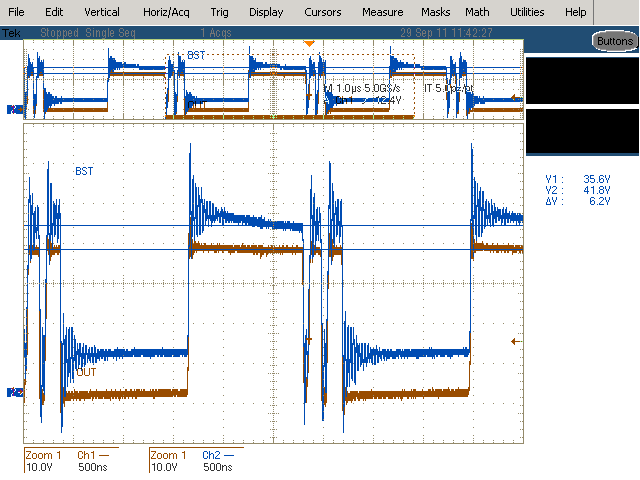
The data sheet states that the UVLO for the bootstrap supply shuts down the half bridge affected, and does not assert the ^SD pin- this is ideal for shutting down C+D half bridges- what is a simple safe way of doing this?

I thought of leaving off Cboot for each half bridge? Or tying boot pin to output with resistor so it is never higher than Vout?

Any help appreciated, I want to commit to pcb soon to try above, better if someone knows though!

regards

  • Can any of the TI guys help on this??

  • Hi Anthony,

    Sorry for not getting back to you as quickly as possible. The way the bootstrap UVLO works is that it detects the voltage delta between OUT and BST.  If that delta reaches a threshold, the OUT line will go low in order to charge the bootstrap cap. After the cap is charged it will resume normal modulation after a few cycles. The BST UVLO is meant to protect against a failing cap or any accidental shorts. (short time). Tying a low resistance from OUT to BST will create a short which will bypass the BST cap which will damaged the device. I actually do UVLO protection and tying a resistive short is how I test for its functionality. Here is a picture of how it works.


     As for pulling out the bootstrap caps, I have not tried that. I can get that tested as soon as possible. I also would like to ask you for some other details.

    1. What kind of load(s) will you be using?

    2. Have you selected what kind of output filter you will be using?

    3. What are the current restrictions of the system? 

    Regards,

    Jay

  • Hi Anthony,

    I just tested the TAS5613 by removing the BST caps and sure enough it damaged the device. I kind of expected this to happen mainly in part because the high side gate isn' t being driven properly. I went ahead and did some quick tests which may help you make a decision.

    The first test I ran the TAS5613 in BTL mode to 10W with dual 4 Ohm loads and checked the current cnnsumption on PVDD. The second test had the device in PBTL mode pushing a single 4 ohm load and checked that current consumption. Here are the numbers I got.

    Note: These numbers are not official or guaranteed but they can give you an idea of what numbers you can see.


    If you use the device in PBTL you will be able to see some lower current consumption. But the draw back is that you will have two slightly different PCBs. I did sketch a quick idea that I think may work for both modes. 


    You would have to route your PCB as you see fit but you can incorporate different mode functionality with these jumpers. The important thing is to make sure the jumpers are rated for the appropriate amount of power. It will also allow for better flexibility.

    Regards,

    Jay

  • The application is a battery backed amplifier for emergency use, I dont want to switch between dual BTL and PBTL; I want to lay the board for PBTL only, and omit the filter components on C+D when we want the low power solution;

    As it is battery powered, I wanted the lowest idle power, and the option of shutting down C+D using BST UVLO looked good.

    When you removed BST cap, did you have a filter on the output? I dont intend to; but also would like to avoid haveing a trace acting as an antena all the way to the vacant filter positions.

    I don't understand how removing the cap failed the device, if the UVLO is meant to protect the device should this happen?

    Can I use a high value bleed resistor to keep uvlo active? if leakage current is 3mA then effective pull down for 3mA is 4K, so if I use 4K resistor VBST can never exceed 6V and should keep it in lock out?

    Thanks for your help so far

    Anthony

  • Load for model A is 50W RMS, Load for model B is 100W RMS supply between 28V and 22V

    Both loads are through 100V line step up transformers, primaries are 12VRMS.

    The transformers are DC protected using 2200u caps bypassed by 10R resistors to prevent large currents on clipping.

    Mode is BD, but with a CM choke before a class AD filter arrangement, reducing idle current considerably.

    System is meant to be battery backed so any savings on idle current will translate to less lead in the rack- a good thing!

  • I did have a filter on the output when I ran the device without the BST caps. The device was damaged when I tested it without the caps but half bridges A, B, and C were still functional. I also pushed the device to full power (without BST caps on C & D) which may have stressed half bridge D too much. UVLO is designed to protect the device but pushing full power for an extended period of time, in a condition in which the device is not designed to run in, will damage it.

    As for the bleed resistor it is the same way I usually test for BST UVLO. The wave form in the post above shows how the device will behave with a bleed resistor (100 ohm power resistor). 

    I would go with the solution above where you operate the device in PBTL and BTL or try using the device in PBTL but place jumpers on OUT C & D very close to the device. (To minimize EMI)  You can remove it for low power, and place it for the higher power.  The half bridges will still be switching but it shouldn’t draw a lot of current.

    You can also use some different setups.

    1.       You can use two devices the TAS5613A and the TAS5611A which are pin to pin compatible.  The TAS5611A is a lower power device which can be used for the low power setup.

    2.       You can also use a TAS5352DDV which is a digital input device but, you can pair it with a PCM1808 to convert the analog input. You would be able to what you want with this set up. The TAS5352 has a RESET_AB and RESET_CD so you would be able to safely shut down the other two half bridges.


  • Thanks for that, I think on rev 1 I may risk a device and try not fitting filter or bst caps; I have also added 0R links near device to isolate tracks should I need to add BST caps.

    According to spec, when switching each 1/2 bridge consumes 10mA gate drive and 12.5mA into filter- this is quite a lot of the overall current consumption.

    I have tried one of the digital modulators with seperate resets, unfortunately this forces /SD high masking other problems.

    What do the reserved modes do on this chip- do you have details?

    I have gone for TAS5613 as I may use on unregulated psu which may reach 33V and the safey net of higher voltage capability appeals; however as Iq is lower on tas5611 it may win out!

  • The reserved modes are usually for testing but I don't know the exact details of them. Which modulator with power stage did you check out?

    Regards,

    Jay

  • is a chart available for Roc vs protect level for the TAS5613A and TAS5611A? the data sheet only gives values for high current- I need to set OC limit to ~6A to protect coils I am using (HA4158 dual 10u coils from coilcraft- low loss for compact class D)

    regards

  • The power stage I used was the TAS5142- I did not use the modulator, I made my own self oscillating amplifier with a comparator ahead of the unit. the performance was exceptional, but licensing issues with NXP lead me to drop the device.

    regards

  • Hi Anthony,

    If I remeber correctly any Roc value above 47K is latching. I believe that for non latching OC protection the lowest limit is a little less than 11 A. But as you said it is a emergency battery powered application so pushing that much power may not be an issue.

    Regards,

    Jacob