This thread has been locked.

If you have a related question, please click the "Ask a related question" button in the top right corner. The newly created question will be automatically linked to this question.

TPA3118D2: Producing lots of heat except when in Sync Slave Configuration

Part Number: TPA3118D2

Tool/software:

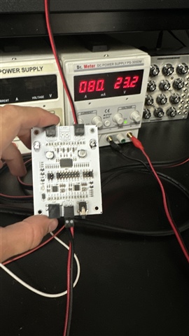
Hi, I have a design using the TPA3118D2 class D amplifier chip. The design is configured with mulitple chips as daughter cards, and a motherboard where they can be connected with one design as the master timing source and 3 other devices as the slaves for sync mode. 

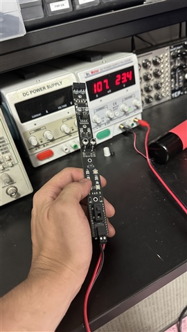
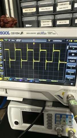
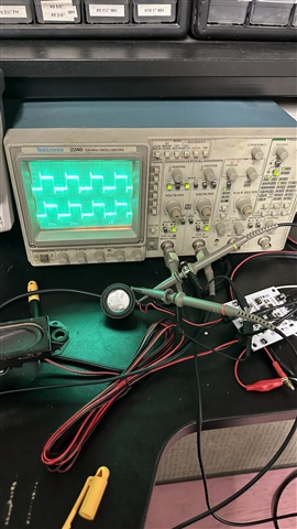
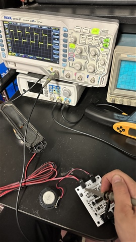
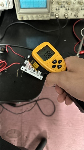
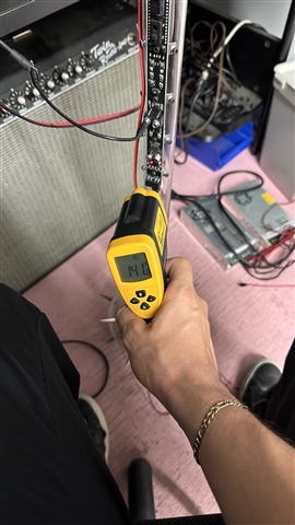
I notice that the master devices gets very hot, whether or not a speaker is plugged in, whereas the slave devices stay cool, regardless of whether a speaker is plugged in. This also occurs when I am using a single chip by itself, as this is used in timing master configuration. The master devices still work and the audio sounds fine, but I would like to eliminate this excessive heat from my design if possible. 

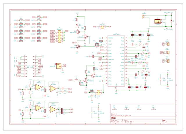
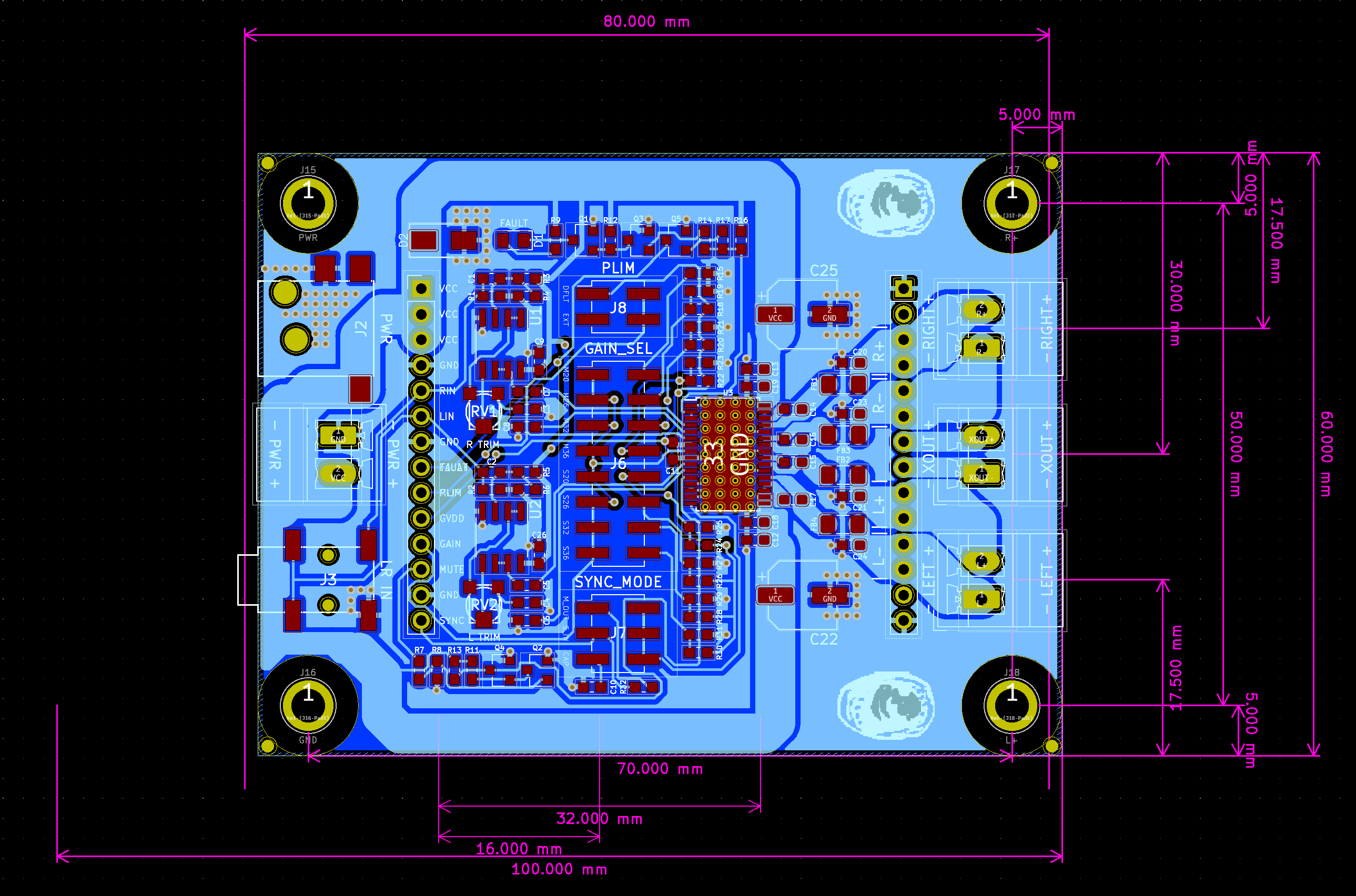
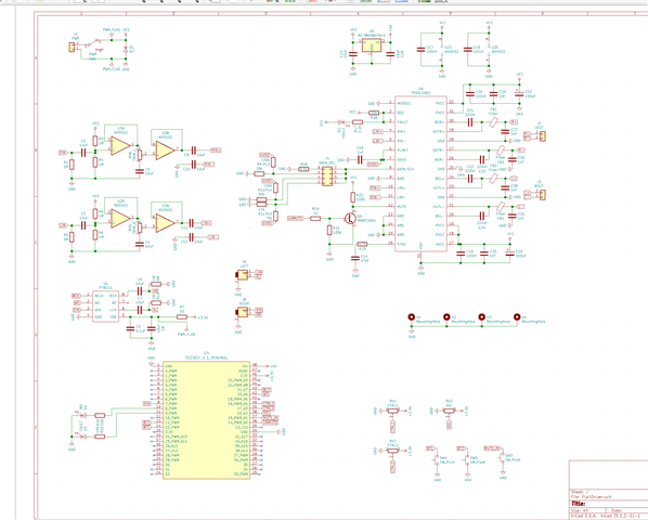
Is there some sort of layout or schematic issue that might be causing this?

Please find my design schematic and layout attached. You can also view the complete KiCad project for my design here: github.com/.../V2.0

  • Hi Emmett,

    C10 should be on the order of pF. The value of this cap used in the datahsheet schematic a typo as explained in this e2e thread (https://e2e.ti.com/support/audio-group/audio/f/audio-forum/732327/tpa3116d2-sync-functionality-issue). Since you are using 4 devices, you would want to use a 15pF cap (or even remove it) since they will all be on the same net.

    From what I can see in the layout image, your ground plane on the top layer is mostly cut off from the device. This means that there is less copper for the device to dissipate heat to. Pages 40 and 41 of the datasheet show a good layout for this device.

    Given the jumpers in this design, you can also try to lower the gain to see if that improves the thermals.

    Regards,

    Ramsey

  • Thank you for this suggestion! I think this may indeed be an issue with the capacitor value, since it seems to be specifically tied master mode being used, and I only have the cap connected for master devices. The slave units don't get excessively hot regardless of gain settings.

    How is the capacitor value for sync calculated and what is its function? It seems like you are saying that I can remove the cap entirely when syncing multiple units? Can I remove the cap when only using a single unit by itself?

    Will be testing the capacitor change when I am back at my bench, but this information would be helpful in the meantime so I can plan out stuff to try. 

  • HI Emmett,

    There is not an exact calculation. The 10K resistor and 1nF cap in the datasheet is used to help reduce overshoot for the slave devices down the line. However, 1nF was too large a value and 47pF is recommended. If you are using one master and 3 slave devices, then the capacitance should be lowered further if you put a cap at each device since they will all be in parallel. The other way would be to just have one 47pF cap near the master (in addition to the 10k Resistor) then no capacitors on the rest of the devices.

    Regards

    Ramsey

  • Is a capacitor necessary if no slave devices are used? Can I simply leave this pin floating in designs where no sync connectivity will be used?

  • Hi Emmett,

    I would recommend still having the RC network on the output in this use case.

    Regards,

    Ransey

  • Okay, and which value for no sync? Like 15pf?

  • Hi Emmett,

    The total capacitance for the RC network should be about 47pF. If no synced devices or one device, use a 47pF capacitor. For multiple synced devices, use either a single 47pF capacitor near the master, or multiple smaller values near each synced device.

    Regards,

    Ramsey

  • Got it, thank you. I'll try replacing C10 with a 47pf and go from there 

  • Hey I now realize I have a different design using one chip with a 10k resistor to a 47pf cap to ground on the sync pin:

    https://github.com/hhaudio/FlailDriver/tree/bigger-reg

    This design still gets very hot, even with nothing plugged in to either output. What might be causing this?

    Here is a photo of the design in use, which should a pretty high static current draw ~100mA at VCC = 24V:

    Does this point to anything in particular? It seems related to the issue I was experiencing on the other design since both display similar behavior

  • Hi Emmett,

    Ramsey is out of office today. He will look into this on Monday. Thank you for your patience.

  • No problem, thanks so much for your support

  • Hi Emmett,

    100mA for the device itself would be higher than expected but given the microcontroller and other devices on the board this seems to be reasonable. The device will protect itself from getting too hot (to where it will damage itself). However, that board does not look to have much area for the heat to escape from so it is likely that the thermals will be hotter due to this. Going back to your original question, can you tell me what the temperature of the devices are and also probe the PWM outputs of the devices?

    Regards,

    Ramsey

  • Hi, I am acquiring a ir thermometer to take accurate heat measurements and will take scope measurements of the PWM signal tomorrow when I am back at the bench. 

    As far as layout goes this is a compact design so the tight form factor cannot be avoided. Would adding 2 additional layers with a solid copper ground planes potentially help with the heat issues? Currently I am using an adhesive heatsink on the back of the board opposite the amplifier chip and a bunch of thermal vias connecting the ground plane under the chip to the other side of the board. 

    Either way I still think there is some schematic / part selection issue going on, since in my other design the chips not generating sync signal don't get hot, while the one generating the clock does. The parts not generating sync are completely cool to the touch so I'd like to get to the bottom of that before making additional changes.

    One thought I had is that ferrite bead selection might be the issue? These are really hard to source since the specifications / ratings for them are extremely unclear in most documentation. I'm never sure which of the ratings are relevant to the design and whether seemingly interchangeable parts will cause problems. Is there anything there I should look into?

    Also, are there any particular points in the circuit you would like me to probe? Also should I take that measurement with a speaker connected or no speaker? Audio playing or no audio?

  • Hi Emmett,

    Ferrite beads tend to cause higher temperatures due to the higher ripple current, and the clock generation could burn some power as well. The amps getting hot is not much of a concern since they will protect themselves and OTSD kicks in at 150C which is well beyond where they feel hot to the touch. The measurements should be taken with a load connected and no audio but the device playing (mute). 

    Regards,

    Ramsey

  • Hi Ramsey, I had the chance to take some measurements. The PWM outputs appear normal on both boards other than a large amount of ripple, the outputs also look to be in correct phase with one another when viewed side by side. The output looks the same at each pin and stays the same whether or not a speaker is plugged in. The static current draw for the larger PCB is around 80mA, removing the sync cap brings it down to 78mA and does not have a noticeable effect on temperature. The larger board sits around 138.5 Fahrenheit, the smaller board sits around 142 Fahrenheit.

    All measurements were taken with a 24V supply, no audio playing. As I said I tested both with and without the speakers plugged in and the measurements looked the same.

    Does this point to anything in particular? This seems like a high temperature / current draw for settings where no audio is being played.

  • Hi Emmett,

    60C is about expected, especially with the limited thermal design mentioned before. Adding snubbers on the outputs could help a bit by helping to damp those overshoots on the PWM as described in this app note. https://www.ti.com/lit/an/sloa201/sloa201.pdf?ts=1723133194059&ref_url=https%253A%252F%252Fwww.google.com%252F 

    Regards,

    Ramsey

  • 60C is expected even with nothing plugged into the device? That seems like a lot of heat to be generated for such a small amount of current, and a very high resting temperature when the amplifier is not even being used. 

    Would switching this to a 4 layer design with 2 additional ground planes for heat sinking (including one on the backside of the board connected to the front by thermal vias) help with the heat issue? Trying to find solutions I can use to improve this without totally changing the form factor.

    For the snubber circuit, will that help reduce the heat, or just the ringing? Where in the output circuit I am using would you recommend inserting a snubber? And what values for the resistor and capacitor?

  • HI Emmett,

    Given the restricted heating layout, the device is likely self heating to this level. It is similar to running an amp with an insufficient heat sink. Adding additional ground layers (especially a backside one) can greatly help this effect. Adding a heat sink on the back side to the copper can also help. Snubbers would help with the ringing which can help marginally with heat dissipation as there would be less overshoot. This would be added at the PWM outputs before the output filter. This Developer's guide can help with designing a snubber. https://www.ti.com/lit/an/sloa201/sloa201.pdf?ts=1723502514030&ref_url=https%253A%252F%252Fwww.google.com%252F 

    Regards,

    Ramsey