This thread has been locked.

If you have a related question, please click the "Ask a related question" button in the top right corner. The newly created question will be automatically linked to this question.

TPA6132A2: Connecting PWM Output from a Class D Amplifier to TPA6132 for Audio Recording and FFT Analysis: Addressing Clipping Issues

Part Number: TPA6132A2
Other Parts Discussed in Thread: TLV320ADC5140, TPA6120A2

Tool/software:

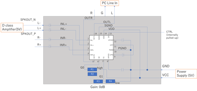
I currently have a mono audio digital signal from an MCU, then it will output as PWM signals (SPKOUT_P and SPKOUT_N ) through a Class D amplifier. Since   the digital signal from the MCU is mono and we are only using the left channel output of the amplifier. I would like to know how to connect the TPA6132 to send these two PWM signals to a PC for recording audio and analysis fft waveform.

My current approach is to connect SPKOUT_P and SPKOUT_N to the INL- and INL+ of the TPA6132, and then connect the OUTL and GND of the TPA6132 to the L and R of the PC's LINE IN jack. However, I found that the audio waveform processed through FFT on the PC is experiencing clipping.

I would like to ask that if my current connection correct?and how can I avoid clipping?

  • Hey Ronghui,

    Can you please provide a schematic of the entire setup ? 

    Regards,

    Ore. 

  • Sorry, here you are.

  • thanks for the schematic. 

    allow 24hrs for a response. 

    Regards. 

  • Sorry, may I ask what additional information I need to provide?

  • Hey Ronghui,

    Thanks for your patience. So far, this top level schematic looks okay. I would like to confirm the VDD of TPA6132 in use and Vrms/ Vpk-pk of the PWM input signal going into TPA6132. 

    I would also like to confirm if the EVM is in use for your setup or if you can share a full schematic supporting the TPA6132 device and devices around it.

    Regards,

    Ore. 

  • Thanks!

    I'm sorry for the lack of information.
    Here is the full schematic.

  • And sorry again for my lack of knowledge, but since I purchased the board from the market, I'm not very familiar with its usage.
    I just discovered today that EN is not set to high (on the board, EN is defined as ctrl).
    Here is the schematic of that board.

  • Hey Ronghui, 

    Thats is okay I could guide you through your issue. However, I would need enough info to do so. To clarify your statement,  EN is an enable pin that could also act as a shutdown pin for the device. Typically this pin is routed to digital logic high or logic low. Below is a quick description:


    The image you have provided is a layout and not a schematic. The schematic used to create this layout is what I need. Please provide answers to the questions asked about VDD and more info on the input signal going into TPA6132A2. Below is an example of a schematic of this device in use on its EVM:


    Regards,

    Ore.    

  • I'm very sorry that I don't have the schematic diagram for this board, as I purchased it on Amazon and currently I cannot contact the seller.
    I used a tester to check the connections on the board and, based on that, I did my best to draw a schematic diagram, which I hope can serve as a reference for you.
    Additionally, the VDD of the TPA6132A2 is 5V, and the Vpk-pk of the PWM input signal going into the TPA6132 is also 5V.
    And, about the EN pin,  I confirmed using an oscilloscope that it is pulled up internally in this board, so it does not affect the operation of the TPA6132A2.
    Thank you!


  • Hey Ronghui,

    Thanks for this. While I review this schematic and your current setup, please provide a scope capture of the output signal clipping and the input signal going into the device. 

    Regards,

    Ore.  

  • Hey Ronghui, 

    Here is my comment after reviewing the schematic:

    • The charge pump circuitry is missing. CPP and CPN need to be shorted through a 1uF cap. An example can be found in the TI EVM schematic attached to this thread. Below is the info on the charge pump:


    • TI is not responsible for the EVMs non-TI vendors create using a TI part. Based off the DS, the gain can be controlled using G0 and G1 and different combinations generate different gain levels. Attached is the table describing how to determine gain:  

                The voltage limits on those pins is also stated in the DS:


    • The schematic is missing HPVDD and HPVSS connections that also support the charge pump circuitry. Below are guidelines as to how those pins should be connected. 


    Regards,

    Ore.  

  • Here are the captures of input signal and output signal.
    Please refer them to check, thank you.
    input signal
    Input signal

    Output signal

  • Sorry, I didn't have time enough to check all the pins yesterday. Today, I confirmed these pins according to your instructions and found that their connections are fine and consistent with the information you provided.
    However, I'm not quite sure about the capacitance values used between them.

    I have updated the circuit diagram; please confirm it. Thank you!


  • Hey Ronghui, 

    I would go over this data and let you know what I observed. Allow 24-48hrs for a response

    Regards,

    Ore.

  • OK, thank you again for your assistance!

  • Hey Ronghui, 

    Now that I have all this information, I see you are lacking the proper circuitry to allow TPA6132A2 process an analog input signal. Your application is a monitoring application. I suggest passing the PWM signal through a LPF filter to monitor the signal as an analog signal.

    Your top level system would need a LPF on the PWM signal entering and leaving the TPA6132A2 device. I attached an example below:


    Regards,

    Ore.

    Disclaimer: TI assumes no liability for applications assistance or customer product design. Customer is fully responsible for all design decisions.

  • I really appreciate you for your suggestion, I will give it a try!
    However, I would like to ask what the reason is for adding a low pass filter into the input and output of TPA6132A2 ?
    And if so, what kind of low pass filter should I add, and how should I add it?

  • Hey Ronghui, 

    It is common practice to pass a PWM signal through an audio LPF to recover the analog signal within it. The PWM signal is a form of digital signal that contains the analog signal generated from a digital source, your MCU for example. There are many LPF options and applications available to use, however TI doesn't sell LPFs. It would be the customer's choice how to implement an audio LPF.   


    Regards,

    Ore.

  • Thank you for your response!
    The reason for adding an LPF is to better monitor the signal; it is necessary to convert the PWM signal from the input section into an analog signal through the LPF. Is my understanding correct?
    And about the output side, I still do not know what the reason is. Could you please tell me more detail about it?
    I apologize for my lack of knowledge in this, and appreciate your guidance.
    Thank you!

  • Hey Ronghui,

    That is correct. I mentioned earlier the output of TPA6132A2 needs a LPF on its output. Seeing as it is an analog output and not a pwm output, an analog-to-digital converter would be required to process analog signals on your PC instead of a LPF at the output stage of TPA6132A2. That support need is beyond the scope of this thread. If you have questions on ADCs and the I2C and I2S audio interfaces required to process analog audio data on your PC, TI audio provides support through e2e on these parts. 

    You can start from TLV320ADC5140.

    Regards,

    Ore. 

  • Thank you again for your explanation. I think I understand why it's necessary to add an LPF on the input side of TPA6132A2.

    However, I still have two questions, and I apologize for bothering you again.

    1. Regarding the input, I will add a LPF before input side. However, I noticed that the max input voltage is specified as HPVDD + 0.3V, and the max of HPVDD is 1.9V, from TPA6132A2 datasheet. Since my PWM signal is 5V, it will still be 5V after converting to an analog signal (which is greater than 2.2V), I am afraid that if inputting this 5V signal into the TPA6132A2 could cause any issues? Additionally, I am not sure where the 1.9V for HPVDD comes from; could you please explain that to me?


    2. Regarding the output,  just as you mentioned previously, the output of the TPA6132A2 is an analog signal, while I found that the PC's line-in interface also requires an analog signal. So, it should not require any additional conversion and can be directly connected to the PC line in jack for observation, is my understanding correct?

    Thank you again for your assistance!


  • Hey Ronghui, 

    To answer your question,

    1. HPVDD is an internal circuit responsible for the input voltage range of the device. For a HPVDD of about 2Vmax, the Vpkpk input signal must not surpass this range. It is advisable to use the recommended operating conditions for TPA6132. If a signal bigger than this range is used, clipping would occur and possible damage to the device. This input range applies to all analog input terminals of the device. A 5Vpkpk input signal to any terminal is too large given the limits of the DS


    2. that is correct.

    I hope I answered all your questions. 

    Regards,

    Ore


  • Sorry for reply later, I was off yesterday. And Thanks for your reply! 
    Oh...Do you mean that I have not been using the TPA6132 under its recommended operating conditions all along, due to the PWM signal 5V voltage is too high? That's really unfortunate...

    There are almost no problem, but please allow me to ask one last question as below.

    So if I want to use the TPA6132, what the condition of analog signal should be?
    Should I first convert a PWM signal into an analog signal using a LPF, and then ensure that the voltage meets the operating conditions of the TPA6132? If so, the upper voltage limit, as mentioned in the datasheet, is 2.2V. Could you please tell me what the lower voltage limit is?

  • The TPA6132 would need an analog signal. So if you have a PWM signal, convert it to analog and then use it on the device. The DS doesn't account for any application regarding direct PWM input signals. 

    The input conditions are in the DS, do not pass these limits

    Regards,

    Ore.

  • I understand. Thank you for the information.

    So, this means that if there is a 5V signal, I shouldn't use the TPA6132, correct? If so, do you have any recommended ICs that I could use?

    Additionally, I tried reducing the output voltage of the amplifier to 3.3V, the PWM signal voltage ranges from 0 to 3.3V.

    After passing through the Input Coupling Capacitors, it becomes approximately -1.5V to 1.8V.

    Would this meet the input requirements of the TPA6132? (I understand that it still needs to be converted to an analog signal using an LPF, but for now, please allow me to discuss the voltage range).
    Thank you again for your kind assistance.

  • As long as the input signal is above approximately 2.2Vpkpk it is not recommended. 

    I would recommend TPA6120A2 instead, it can accommodate wider signals. 

    Regards.

  • Thank you for your kind assistance.
    I have no problem now!
    And thanks again for your recommendation!