


Hi,
1. I am trying to set a 4th-order notch filter using Pure Path using the cascaded biquads block.
I was able to make this filter work for primary AIS interface of tlv320aic3254 chip. Attched below are Mag vs frequency responses of
recorded audio on primary interface.
Without Notch Filter :
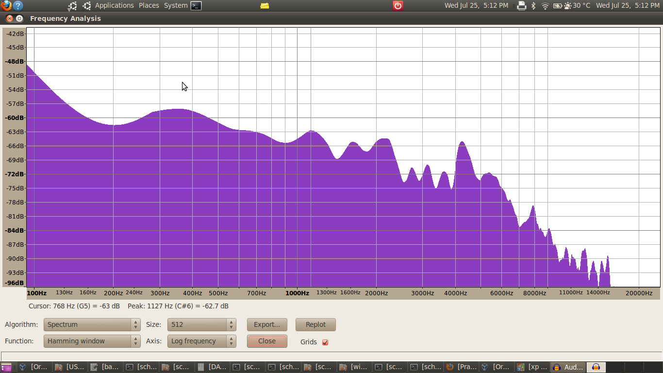
With Notch Filter at 4.2Khz:
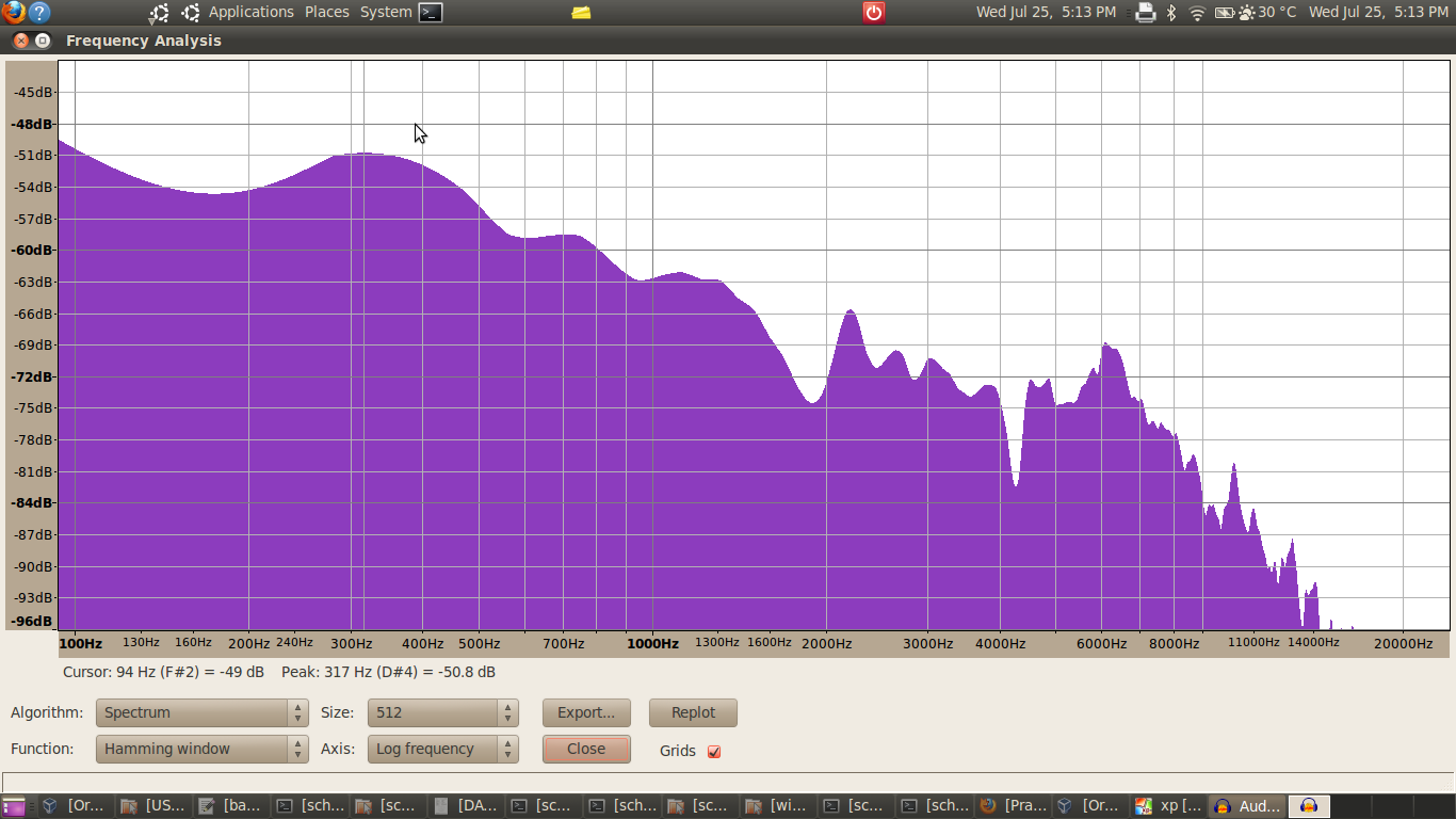
2. I have trouble getting this filter work for the Secondary AIS interface of tlv320aic3254.
I do get audio on this Interface, but the frequency response shows that the filtering action has not taken place !!!
i.e. I don't see a dip at 4.2Khz in the Mag vs Frequency response.
3. I have no clue as what is going wrong.
I have attached the Pure Path text scripts (which I have modified to suit my hardware) using for primary and secondary AIS interface.
;-----------------------------------------------------------------------------------
; Software Reset
;-----------------------------------------------------------------------------------
    reg[  0][  1] = 0x01    ; Initialize the device through software reset
       reg[254][  0] = 0x0a    ; Delay 10ms

;-----------------------------------------------------------------------------------
; Configure Power Supplies
;-----------------------------------------------------------------------------------
    %%if (%%prop(TargetBoard) == 2)
; AIC3254EVM-U specific configuration

    reg[  1][  2] = 0xa9    ; Power up AVDD LDO
    reg[  1][  1] = 0x08    ; Disable weak AVDD to DVDD connection
    reg[  1][  2] = 0xa1    ; Enable Master Analog Power Control, AVDD LDO Powered

    %%else
; AIC3254EVM-K specific configuration
    reg[  1][  2] = 0x09    ; Disable weak AVDD to DVDD connection
    reg[  1][  1] = 0x08    ; Enable Master Analog Power Control
    reg[  1][  2] = 0x01    ; Disable weak AVDD to DVDD connection

    %%endif

    reg[  1][ 71] = 0x32    ; Set the input power-up time to 3.1ms
    reg[  1][123] = 0x01    ; Set REF charging time to 40ms (automatic)
;    reg[254][0] = 0x28    ; Delay 40ms for REF to Power Up

;-----------------------------------------------------------------------------------
; Load miniDSP Code
;-----------------------------------------------------------------------------------
    PROGRAM_ADC        ; miniDSP_A coefficients and instructions
    PROGRAM_DAC        ; miniDSP_D coefficients and instructions

;-----------------------------------------------------------------------------------
; Signal Processing Settings
;-----------------------------------------------------------------------------------
%%if (%%prop(SynchMode) == 1)
    ; SynchMode is enabled
    reg[  0][ 60] = 0x80    ; DAC prog Mode: miniDSP_A and miniDSP_D ARE powered up together, miniDSP_A used for signal processing
%%else
    ; SynchMode is disabled
    reg[  0][ 60] = 0x00    ; DAC prog Mode: miniDSP_A and miniDSP_D NOT powered up together, miniDSP_A used for signal processing
%%endif
    reg[  0][ 61] = 0x00    ; Use miniDSP_A for signal processing

    %%if ("%%prop(FrameworkType)" == "AIC3254App8x4x")
    reg[  0][ 17] = 0x08    ; 8x Interpolation
    reg[  0][ 23] = 0x04    ; 4x Decimation
    %%endif

    %%if ("%%prop(FrameworkType)" == "AIC3254App4x2x")
    reg[  0][ 17] = 0x04    ; 4x Interpolation
    reg[  0][ 23] = 0x02    ; 2x Decimation
    %%endif

    %%if ("%%prop(FrameworkType)" == "AIC3254App2x1x")
    reg[  0][ 17] = 0x02    ; 2x Interpolation
    reg[  0][ 23] = 0x01    ; 1x Decimation
    %%endif

    IDAC  = %%prop(miniDSP_D_Cycles)
    IADC  = %%prop(miniDSP_A_Cycles)

    %%if (%%prop(miniDSP_A_Adaptive) == 1)
    reg[  8][  1] = 0x04    ; adaptive mode for ADC
    %%endif

    %%if (%%prop(miniDSP_D_Adaptive) == 1)
    reg[ 44][  1] = 0x04    ; adaptive mode for DAC
    %%endif

;-----------------------------------------------------------------------------------
; Clock and Interface Configuration
;-----------------------------------------------------------------------------------
; USB Audio supports 8kHz to 48kHz sample rates
; An external audio interface is required for 88.2kHz to 192kHz sample rates
;-----------------------------------------------------------------------------------
    %%if (%%prop(SampleRate) == 176400 || %%prop(SampleRate) == 192000)
    reg[  0][  5] = 0x91    ; P=1, R=1, J=8
    reg[  0][  6] = 0x08    ; P=1, R=1, J=8
    reg[  0][  7] = 0x00    ; D=0000 (MSB)
    reg[  0][  8] = 0x00    ; D=0000 (LSB)
    reg[  0][  4] = 0x03    ; PLL_clkin = MCLK, codec_clkin = PLL_CLK, PLL on
    reg[  0][ 12] = 0x88    ; MDAC = 8, divider powered on
    reg[  0][ 13] = 0x00    ; DOSR = 32 (MSB)
    reg[  0][ 14] = 0x20    ; DOSR = 32 (LSB)
    reg[  0][ 18] = 0x02    ; NADC = 2, divider powered off
    reg[  0][ 19] = 0x88    ; MADC = 8, divider powered on
    reg[  0][ 20] = 0x20    ; AOSR = 32
    reg[  0][ 11] = 0x82    ; NDAC = 2, divider powered on

    %%endif

    %%if (%%prop(SampleRate) == 88200 || %%prop(SampleRate) == 96000)
    reg[  0][  5] = 0x91    ; P=1, R=1, J=8
    reg[  0][  6] = 0x08    ; P=1, R=1, J=8
    reg[  0][  7] = 0x00    ; D=0000 (MSB)
    reg[  0][  8] = 0x00    ; D=0000 (LSB)
    reg[  0][  4] = 0x0f    ; PLL_clkin = MCLK, codec_clkin = PLL_CLK, PLL on
    reg[  0][ 12] = 0x88    ; MDAC = 8, divider powered on
    reg[  0][ 13] = 0x00    ; DOSR = 64 (MSB)
    reg[  0][ 14] = 0x40    ; DOSR = 64 (LSB)
    reg[  0][ 18] = 0x02    ; NADC = 2, divider powered off
    reg[  0][ 19] = 0x88    ; MADC = 8, divider powered on
    reg[  0][ 20] = 0x40    ; AOSR = 64
    reg[  0][ 11] = 0x82    ; NDAC = 2, divider powered on
    %%endif

    %%if (%%prop(SampleRate) == 44100 || %%prop(SampleRate) == 48000)
        reg[  0][  5] = 0x91    ; P=1, R=1, J=8
        reg[  0][  6] = 0x08    ; P=1, R=1, J=8
        reg[  0][  7] = 0x00    ; D=0000 (MSB)
        reg[  0][  8] = 0x00    ; D=0000 (LSB)
        reg[  0][  4] = 0x0f    ; PLL_clkin = MCLK, codec_clkin = PLL_CLK, PLL on
        reg[  0][ 12] = 0x88    ; MDAC = 8, divider powered on
        reg[  0][ 13] = 0x00    ; DOSR = 128 (MSB)
        reg[  0][ 14] = 0x80    ; DOSR = 128 (LSB)
        reg[  0][ 18] = 0x02    ; NADC = 2, divider powered off
        reg[  0][ 19] = 0x88    ; MADC = 8, divider powered on
        reg[  0][ 20] = 0x80    ; AOSR = 128
        reg[  0][ 11] = 0x82    ; NDAC = 2, divider powered on
    %%endif

    %%if (%%prop(SampleRate) == 32000)
    reg[  0][  5] = 0x91    ; P=1, R=1, J=8
    reg[  0][  6] = 0x08    ; P=1, R=1, J=8
    reg[  0][  7] = 0x00    ; D=0000 (MSB)
    reg[  0][  8] = 0x00    ; D=0000 (LSB)
    reg[  0][  4] = 0x03    ; PLL_clkin = MCLK, codec_clkin = PLL_CLK, PLL on
    reg[  0][ 12] = 0x88    ; MDAC = 8, divider powered on
    reg[  0][ 13] = 0x00    ; DOSR = 192 (MSB)
    reg[  0][ 14] = 0xc0    ; DOSR = 192 (LSB)
    reg[  0][ 18] = 0x02    ; NADC = 2, divider powered off
    reg[  0][ 19] = 0x8c    ; MADC = 12, divider powered on
    reg[  0][ 20] = 0x80    ; AOSR = 128
    reg[  0][ 11] = 0x82    ; NDAC = 2, divider powered on
    %%endif

    %%if (%%prop(SampleRate) == 22050 || %%prop(SampleRate) == 24000)
    reg[  0][  5] = 0x91    ; P=1, R=1, J=8
    reg[  0][  6] = 0x08    ; P=1, R=1, J=8
    reg[  0][  7] = 0x00    ; D=0000 (MSB)
    reg[  0][  8] = 0x00    ; D=0000 (LSB)
    reg[  0][  4] = 0x03    ; PLL_clkin = MCLK, codec_clkin = PLL_CLK, PLL on
    reg[  0][ 12] = 0x88    ; MDAC = 8, divider powered on
    reg[  0][ 13] = 0x01    ; DOSR = 256 (MSB)
    reg[  0][ 14] = 0x00    ; DOSR = 256 (LSB)
    reg[  0][ 18] = 0x02    ; NADC = 2, divider powered off
    reg[  0][ 19] = 0x90    ; MADC = 16, divider powered on
    reg[  0][ 20] = 0x80    ; AOSR = 128
    reg[  0][ 11] = 0x82    ; NDAC = 2, divider powered on
    %%endif

    %%if (%%prop(SampleRate) == 16000)
    reg[  0][  5] = 0x91    ; P=1, R=1, J=24
    reg[  0][  6] = 0x18    ; P=1, R=1, J=24
    reg[  0][  7] = 0x00    ; D=0000 (MSB)
    reg[  0][  8] = 0x00    ; D=0000 (LSB)
    reg[  0][  4] = 0x03    ; PLL_clkin = MCLK, codec_clkin = PLL_CLK, PLL on
    reg[  0][ 12] = 0x88    ; MDAC = 8, divider powered on
    reg[  0][ 13] = 0x01    ; DOSR = 384 (MSB)
    reg[  0][ 14] = 0x80    ; DOSR = 384 (LSB)
    reg[  0][ 18] = 0x02    ; NADC = 2, divider powered off
    reg[  0][ 19] = 0x98    ; MADC = 24, divider powered on
    reg[  0][ 20] = 0x80    ; AOSR = 128
    reg[  0][ 11] = 0x82    ; NDAC = 2, divider powered on
    %%endif

    %%if (%%prop(SampleRate) == 11025)
    reg[  0][  5] = 0x91    ; P=1, R=1, J=16
    reg[  0][  6] = 0x10    ; P=1, R=1, J=16
    reg[  0][  7] = 0x00    ; D=0000 (MSB)
    reg[  0][  8] = 0x00    ; D=0000 (LSB)
    reg[  0][  4] = 0x03    ; PLL_clkin = MCLK, codec_clkin = PLL_CLK, PLL on
    reg[  0][ 12] = 0x88    ; MDAC = 8, divider powered on
    reg[  0][ 13] = 0x02    ; DOSR = 512 (MSB)
    reg[  0][ 14] = 0x00    ; DOSR = 512 (LSB)
    reg[  0][ 18] = 0x02    ; NADC = 2, divider powered off
    reg[  0][ 19] = 0xa0    ; MADC = 32, divider powered on
    reg[  0][ 20] = 0x80    ; AOSR = 128
    reg[  0][ 11] = 0x82    ; NDAC = 2, divider powered on
    %%endif

    %%if (%%prop(SampleRate) == 8000)
    reg[  0][  5] = 0x91    ; P=1, R=1, J=24
    reg[  0][  6] = 0x18    ; P=1, R=1, J=24
    reg[  0][  7] = 0x00    ; D=0000 (MSB)
    reg[  0][  8] = 0x00    ; D=0000 (LSB)
    reg[  0][  4] = 0x03    ; PLL_clkin = MCLK, codec_clkin = PLL_CLK, PLL on
    reg[  0][ 12] = 0x88    ; MDAC = 8, divider powered on
    reg[  0][ 13] = 0x03    ; DOSR = 768 (MSB)
    reg[  0][ 14] = 0x00    ; DOSR = 768 (LSB)
    reg[  0][ 18] = 0x02    ; NADC = 2, divider powered off
    reg[  0][ 19] = 0xb0    ; MADC = 48, divider powered on
    reg[  0][ 20] = 0x80    ; AOSR = 128
    reg[  0][ 11] = 0x82    ; NDAC = 2, divider powered on
    %%endif


;-----------------------------------------------------------------------------------
; ADC Channel Configuration
;-----------------------------------------------------------------------------------
      ;reg[  1][ 51] = 0x40    ; Mic Bias enabled, Source = Avdd, 1.25V

    %%if (%%prop(TargetBoard) == 2)
; AIC3254EVM-U specific configuration
    reg[  1][ 52] = 0x10    ; Route IN2L to LEFT_P with 10K input impedance
    reg[  1][ 54] = 0x40    ; Route CM1L to LEFT_M with 10K input impedance
    reg[  1][ 55] = 0x10    ; Route IN2R to RIGHT_P with 10K input impedance

    %%else
; AIC3254EVM-K specific configuration
    reg[  0][ 28] = 0x00    ; Disable weak AVDD to DVDD connection
    reg[  0][ 29] = 0x14    ; Disable weak AVDD to DVDD connection
    reg[  1][ 10] = 0x7b    ; Disable weak AVDD to DVDD connection
    ;reg[  1][  2] = 0x09    ; Disable weak AVDD to DVDD connection
    reg[  1][ 51] = 0x58    ; Disable weak AVDD to DVDD connection
    reg[  1][ 52] = 0x04    ; Route IN1L to LEFT_P with 10K input impedance
    reg[  1][ 54] = 0x04    ; Route CM1L to LEFT_M with 10K input impedance
    reg[  1][ 55] = 0x10    ; Route IN1R to RIGHT_P with 10K input impedance
    reg[  1][ 57] = 0x10    ; Disable weak AVDD to DVDD connection4
    reg[  1][ 59] = 0x35    ; Disable weak AVDD to DVDD connection
    reg[  1][ 60] = 0x35    ; Disable weak AVDD to DVDD connection


    %%endif

    ;reg[  1][ 57] = 0x40    ; Route CM1R to RIGHT_M with 10K input impedance
    ;reg[  1][ 59] = 0x35    ; Enable MicPGA_L Gain Control, 0dB
    ;reg[  1][ 60] = 0x00    ; Enable MicPGA_R Gain Control, 0dB
    reg[  0][ 81] = 0xc0    ; Power up LADC/RADC
    reg[  0][ 82] = 0x00    ; Unmute LADC/RADC


;-----------------------------------------------------------------------------------
; DAC Channel Configuration
;-----------------------------------------------------------------------------------
;-----------------------------------------------------------------------------------
; Software Reset
;-----------------------------------------------------------------------------------
    reg[  0][  1] = 0x01    ; Initialize the device through software reset
       reg[254][  0] = 0x0a    ; Delay 10ms

;-----------------------------------------------------------------------------------
; Configure Power Supplies
;-----------------------------------------------------------------------------------
    %%if (%%prop(TargetBoard) == 2)
; AIC3254EVM-U specific configuration

    reg[  1][  2] = 0xa9    ; Power up AVDD LDO
    reg[  1][  1] = 0x08    ; Disable weak AVDD to DVDD connection
    reg[  1][  2] = 0xa1    ; Enable Master Analog Power Control, AVDD LDO Powered

    %%else
; AIC3254EVM-K specific configuration
    reg[  1][  2] = 0x09    ; Disable weak AVDD to DVDD connection
    reg[  1][  1] = 0x08    ; Enable Master Analog Power Control
    reg[  1][  2] = 0x01    ; Disable weak AVDD to DVDD connection

    %%endif

    reg[  1][ 71] = 0x32    ; Set the input power-up time to 3.1ms
    reg[  1][123] = 0x01    ; Set REF charging time to 40ms (automatic)
;    reg[254][0] = 0x28    ; Delay 40ms for REF to Power Up

;-----------------------------------------------------------------------------------
; Load miniDSP Code
;-----------------------------------------------------------------------------------
    PROGRAM_ADC        ; miniDSP_A coefficients and instructions
    PROGRAM_DAC        ; miniDSP_D coefficients and instructions

;-----------------------------------------------------------------------------------
; Signal Processing Settings
;-----------------------------------------------------------------------------------
%%if (%%prop(SynchMode) == 1)
    ; SynchMode is enabled
    reg[  0][ 60] = 0x80    ; DAC prog Mode: miniDSP_A and miniDSP_D ARE powered up together, miniDSP_A used for signal processing
%%else
    ; SynchMode is disabled
    reg[  0][ 60] = 0x00    ; DAC prog Mode: miniDSP_A and miniDSP_D NOT powered up together, miniDSP_A used for signal processing
%%endif
    reg[  0][ 61] = 0x00    ; Use miniDSP_A for signal processing

    %%if ("%%prop(FrameworkType)" == "AIC3254App8x4x")
    reg[  0][ 17] = 0x08    ; 8x Interpolation
    reg[  0][ 23] = 0x04    ; 4x Decimation
    %%endif

    %%if ("%%prop(FrameworkType)" == "AIC3254App4x2x")
    reg[  0][ 17] = 0x04    ; 4x Interpolation
    reg[  0][ 23] = 0x02    ; 2x Decimation
    %%endif

    %%if ("%%prop(FrameworkType)" == "AIC3254App2x1x")
    reg[  0][ 17] = 0x02    ; 2x Interpolation
    reg[  0][ 23] = 0x01    ; 1x Decimation
    %%endif

    IDAC  = %%prop(miniDSP_D_Cycles)
    IADC  = %%prop(miniDSP_A_Cycles)

    %%if (%%prop(miniDSP_A_Adaptive) == 1)
    reg[  8][  1] = 0x04    ; adaptive mode for ADC
    %%endif

    %%if (%%prop(miniDSP_D_Adaptive) == 1)
    reg[ 44][  1] = 0x04    ; adaptive mode for DAC
    %%endif

;-----------------------------------------------------------------------------------
; Clock and Interface Configuration
;-----------------------------------------------------------------------------------
; USB Audio supports 8kHz to 48kHz sample rates
; An external audio interface is required for 88.2kHz to 192kHz sample rates
;-----------------------------------------------------------------------------------
    %%if (%%prop(SampleRate) == 176400 || %%prop(SampleRate) == 192000)
    reg[  0][  5] = 0x91    ; P=1, R=1, J=8
    reg[  0][  6] = 0x08    ; P=1, R=1, J=8
    reg[  0][  7] = 0x00    ; D=0000 (MSB)
    reg[  0][  8] = 0x00    ; D=0000 (LSB)
    reg[  0][  4] = 0x03    ; PLL_clkin = MCLK, codec_clkin = PLL_CLK, PLL on
    reg[  0][ 12] = 0x88    ; MDAC = 8, divider powered on
    reg[  0][ 13] = 0x00    ; DOSR = 32 (MSB)
    reg[  0][ 14] = 0x20    ; DOSR = 32 (LSB)
    reg[  0][ 18] = 0x02    ; NADC = 2, divider powered off
    reg[  0][ 19] = 0x88    ; MADC = 8, divider powered on
    reg[  0][ 20] = 0x20    ; AOSR = 32
    reg[  0][ 11] = 0x82    ; NDAC = 2, divider powered on

    %%endif

    %%if (%%prop(SampleRate) == 88200 || %%prop(SampleRate) == 96000)
    reg[  0][  5] = 0x91    ; P=1, R=1, J=8
    reg[  0][  6] = 0x08    ; P=1, R=1, J=8
    reg[  0][  7] = 0x00    ; D=0000 (MSB)
    reg[  0][  8] = 0x00    ; D=0000 (LSB)
    reg[  0][  4] = 0x0f    ; PLL_clkin = MCLK, codec_clkin = PLL_CLK, PLL on
    reg[  0][ 12] = 0x88    ; MDAC = 8, divider powered on
    reg[  0][ 13] = 0x00    ; DOSR = 64 (MSB)
    reg[  0][ 14] = 0x40    ; DOSR = 64 (LSB)
    reg[  0][ 18] = 0x02    ; NADC = 2, divider powered off
    reg[  0][ 19] = 0x88    ; MADC = 8, divider powered on
    reg[  0][ 20] = 0x40    ; AOSR = 64
    reg[  0][ 11] = 0x82    ; NDAC = 2, divider powered on
    %%endif

    %%if (%%prop(SampleRate) == 44100 || %%prop(SampleRate) == 48000)
        reg[  0][  5] = 0x91    ; P=1, R=1, J=8
        reg[  0][  6] = 0x08    ; P=1, R=1, J=8
        reg[  0][  7] = 0x00    ; D=0000 (MSB)
        reg[  0][  8] = 0x00    ; D=0000 (LSB)
        reg[  0][  4] = 0x0f    ; PLL_clkin = MCLK, codec_clkin = PLL_CLK, PLL on
        reg[  0][ 12] = 0x88    ; MDAC = 8, divider powered on
        reg[  0][ 13] = 0x00    ; DOSR = 128 (MSB)
        reg[  0][ 14] = 0x80    ; DOSR = 128 (LSB)
        reg[  0][ 18] = 0x02    ; NADC = 2, divider powered off
        reg[  0][ 19] = 0x88    ; MADC = 8, divider powered on
        reg[  0][ 20] = 0x80    ; AOSR = 128
        reg[  0][ 11] = 0x82    ; NDAC = 2, divider powered on
    %%endif

    %%if (%%prop(SampleRate) == 32000)
    reg[  0][  5] = 0x91    ; P=1, R=1, J=8
    reg[  0][  6] = 0x08    ; P=1, R=1, J=8
    reg[  0][  7] = 0x00    ; D=0000 (MSB)
    reg[  0][  8] = 0x00    ; D=0000 (LSB)
    reg[  0][  4] = 0x03    ; PLL_clkin = MCLK, codec_clkin = PLL_CLK, PLL on
    reg[  0][ 12] = 0x88    ; MDAC = 8, divider powered on
    reg[  0][ 13] = 0x00    ; DOSR = 192 (MSB)
    reg[  0][ 14] = 0xc0    ; DOSR = 192 (LSB)
    reg[  0][ 18] = 0x02    ; NADC = 2, divider powered off
    reg[  0][ 19] = 0x8c    ; MADC = 12, divider powered on
    reg[  0][ 20] = 0x80    ; AOSR = 128
    reg[  0][ 11] = 0x82    ; NDAC = 2, divider powered on
    %%endif

    %%if (%%prop(SampleRate) == 22050 || %%prop(SampleRate) == 24000)
    reg[  0][  5] = 0x91    ; P=1, R=1, J=8
    reg[  0][  6] = 0x08    ; P=1, R=1, J=8
    reg[  0][  7] = 0x00    ; D=0000 (MSB)
    reg[  0][  8] = 0x00    ; D=0000 (LSB)
    reg[  0][  4] = 0x03    ; PLL_clkin = MCLK, codec_clkin = PLL_CLK, PLL on
    reg[  0][ 12] = 0x88    ; MDAC = 8, divider powered on
    reg[  0][ 13] = 0x01    ; DOSR = 256 (MSB)
    reg[  0][ 14] = 0x00    ; DOSR = 256 (LSB)
    reg[  0][ 18] = 0x02    ; NADC = 2, divider powered off
    reg[  0][ 19] = 0x90    ; MADC = 16, divider powered on
    reg[  0][ 20] = 0x80    ; AOSR = 128
    reg[  0][ 11] = 0x82    ; NDAC = 2, divider powered on
    %%endif

    %%if (%%prop(SampleRate) == 16000)
    reg[  0][  5] = 0x91    ; P=1, R=1, J=24
    reg[  0][  6] = 0x18    ; P=1, R=1, J=24
    reg[  0][  7] = 0x00    ; D=0000 (MSB)
    reg[  0][  8] = 0x00    ; D=0000 (LSB)
    reg[  0][  4] = 0x03    ; PLL_clkin = MCLK, codec_clkin = PLL_CLK, PLL on
    reg[  0][ 12] = 0x88    ; MDAC = 8, divider powered on
    reg[  0][ 13] = 0x01    ; DOSR = 384 (MSB)
    reg[  0][ 14] = 0x80    ; DOSR = 384 (LSB)
    reg[  0][ 18] = 0x02    ; NADC = 2, divider powered off
    reg[  0][ 19] = 0x98    ; MADC = 24, divider powered on
    reg[  0][ 20] = 0x80    ; AOSR = 128
    reg[  0][ 11] = 0x82    ; NDAC = 2, divider powered on
    %%endif

    %%if (%%prop(SampleRate) == 11025)
    reg[  0][  5] = 0x91    ; P=1, R=1, J=16
    reg[  0][  6] = 0x10    ; P=1, R=1, J=16
    reg[  0][  7] = 0x00    ; D=0000 (MSB)
    reg[  0][  8] = 0x00    ; D=0000 (LSB)
    reg[  0][  4] = 0x03    ; PLL_clkin = MCLK, codec_clkin = PLL_CLK, PLL on
    reg[  0][ 12] = 0x88    ; MDAC = 8, divider powered on
    reg[  0][ 13] = 0x02    ; DOSR = 512 (MSB)
    reg[  0][ 14] = 0x00    ; DOSR = 512 (LSB)
    reg[  0][ 18] = 0x02    ; NADC = 2, divider powered off
    reg[  0][ 19] = 0xa0    ; MADC = 32, divider powered on
    reg[  0][ 20] = 0x80    ; AOSR = 128
    reg[  0][ 11] = 0x82    ; NDAC = 2, divider powered on
    %%endif

    %%if (%%prop(SampleRate) == 8000)
    reg[  0][  5] = 0x91    ; P=1, R=1, J=24
    reg[  0][  6] = 0x18    ; P=1, R=1, J=24
    reg[  0][  7] = 0x00    ; D=0000 (MSB)
    reg[  0][  8] = 0x00    ; D=0000 (LSB)
    reg[  0][  4] = 0x03    ; PLL_clkin = MCLK, codec_clkin = PLL_CLK, PLL on
    reg[  0][ 12] = 0x88    ; MDAC = 8, divider powered on
    reg[  0][ 13] = 0x03    ; DOSR = 768 (MSB)
    reg[  0][ 14] = 0x00    ; DOSR = 768 (LSB)
    reg[  0][ 18] = 0x02    ; NADC = 2, divider powered off
    reg[  0][ 19] = 0xb0    ; MADC = 48, divider powered on
    reg[  0][ 20] = 0x80    ; AOSR = 128
    reg[  0][ 11] = 0x82    ; NDAC = 2, divider powered on
    %%endif


;-----------------------------------------------------------------------------------
; ADC Channel Configuration
;-----------------------------------------------------------------------------------
      ;reg[  1][ 51] = 0x40    ; Mic Bias enabled, Source = Avdd, 1.25V

    %%if (%%prop(TargetBoard) == 2)
; AIC3254EVM-U specific configuration
    reg[  1][ 52] = 0x10    ; Route IN2L to LEFT_P with 10K input impedance
    reg[  1][ 54] = 0x40    ; Route CM1L to LEFT_M with 10K input impedance
    reg[  1][ 55] = 0x10    ; Route IN2R to RIGHT_P with 10K input impedance

    %%else
; AIC3254EVM-K specific configuration
    reg[  0][ 52] = 0x04    ; Seconday Wclk = MFP5
    reg[  0][ 55] = 0x10    ; Secondary Output = MFP4
    reg[  0][ 31] = 0x20    ; Secondary MUX for Wclk = GPIO/MFP5 & Secondary MUX for Bclk = SCLK/MFP3
    reg[  0][ 32] = 0x0e    ; AIS will use secondary interface settings
    reg[  0][ 33] = 0x3d    ; Secondary Data output from Serial Interface
    reg[  0][ 29] = 0x04    ; Force AIS output the respective secondary clks
    reg[  0][ 27] = 0x20    ; 24-Bit format on I2S
    reg[  1][ 10] = 0x7b    ; 0.75 V common mode
    ;reg[  0][ 61] = 0x01    ; Processing block 1 for ADC, IIR with flat response
    ;reg[  1][ 61] = 0x64    ; ADC PowerTuneMode 3
    reg[  1][ 51] = 0x58    ; Mic Bias 1.45 V
    reg[  1][ 52] = 0x10    ; Route IN1L to LEFT_P with 10K input impedance
    reg[  1][ 54] = 0x10    ; Route CM1L to LEFT_M with 10K input impedance
    reg[  1][ 55] = 0x04    ; Route IN1R to RIGHT_P with 10K input impedance
    reg[  1][ 57] = 0x04    ; Disable weak AVDD to DVDD connection4
    reg[  1][ 59] = 0x2a   ; Disable weak AVDD to DVDD connection
    reg[  1][ 60] = 0x2a    ; Disable weak AVDD to DVDD connection


    %%endif

    ;reg[  1][ 57] = 0x40    ; Route CM1R to RIGHT_M with 10K input impedance
    ;reg[  1][ 59] = 0x35    ; Enable MicPGA_L Gain Control, 0dB
    ;reg[  1][ 60] = 0x00    ; Enable MicPGA_R Gain Control, 0dB
    reg[  0][ 81] = 0xc0    ; Power up LADC/RADC
    reg[  0][ 82] = 0x00    ; Unmute LADC/RADC


;-----------------------------------------------------------------------------------
; DAC Channel Configuration
;-----------------------------------------------------------------------------------
Can someone please help in reviewing this script, particularly for the secondary interface.
I am not sure above scripts are sufficient to debug the problem, please do inform if any further details are needed.
Thanks,
Brontok :)


