Hi
We have question of TAS5342LA.
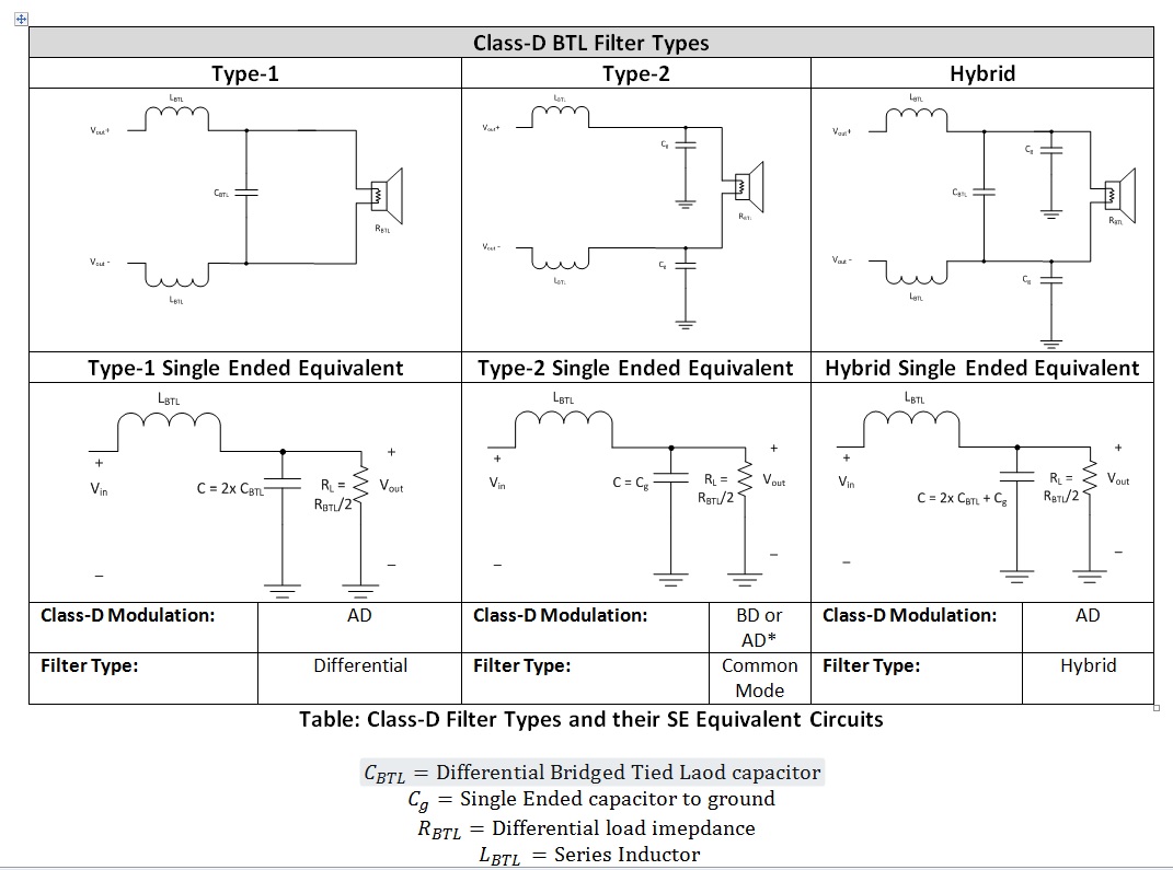
We are going to use this device with BD, but according to datasheet, TAS5342LA had been tested with AD modulation. Also, the reference schematic is described in AD.
1.
Where can we refer the schematic for BD modulation?
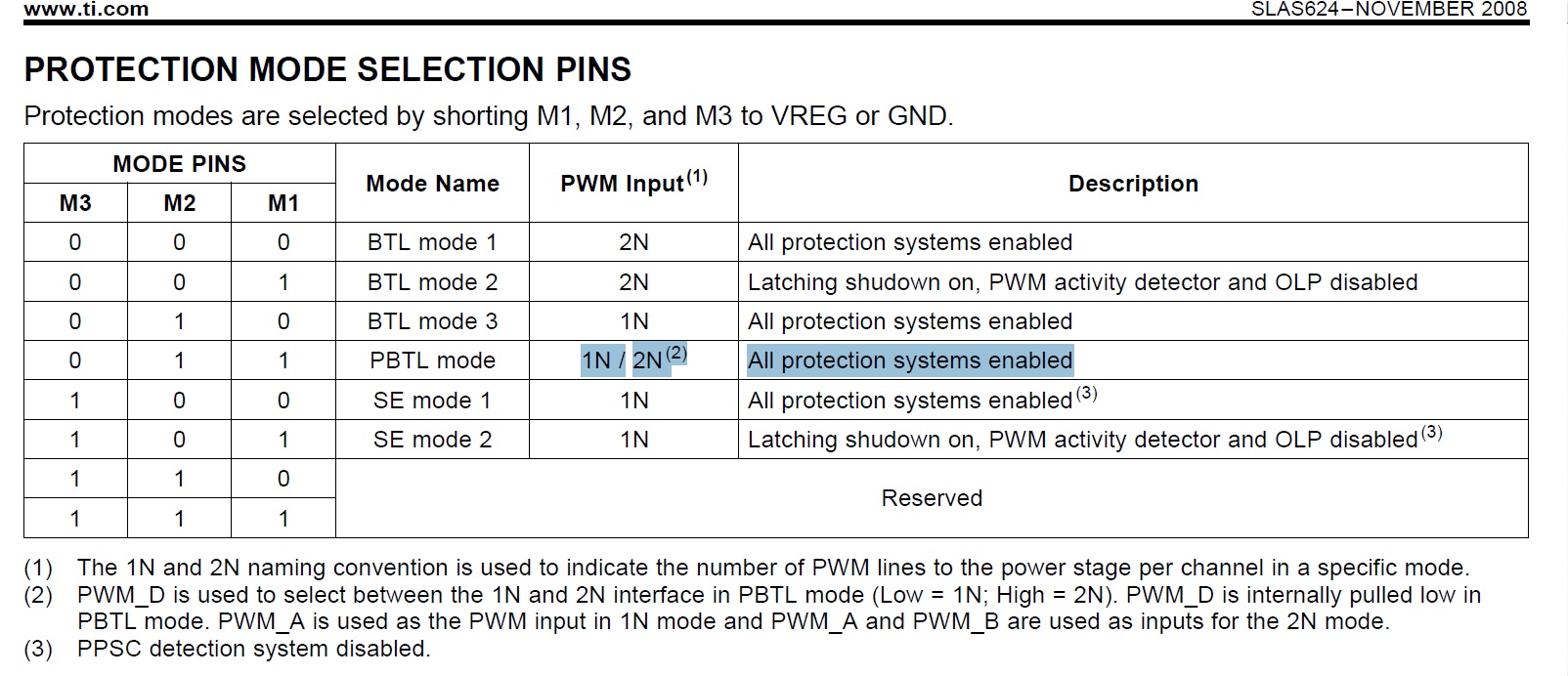
We want to refer 2N BTL and 2N PBTL.
2.
In the figure17 Typical Differential (2N) PBTL application with AD modulation Filters, PWM_C is open and PWM_D is connected to VREG. Can you tell us why it has such termination if you know?
3.
Do you have information about PCB design guideline?
Especially, we want to know the note of caution for the connection of AGND and OC_ADJ if any. We want to avoid failing detection of overcurrent.
4.
OTW and SD have internal pullup register to VREG, so external pullup is not required.
If two device are used, are there problem that we connect OTW to OTW and SD to SD each other?
BestReards