This thread has been locked.

If you have a related question, please click the "Ask a related question" button in the top right corner. The newly created question will be automatically linked to this question.

TAS5414C-Q1: Regarding Input Bias and Common Mode Range

Part Number: TAS5414C-Q1
Other Parts Discussed in Thread: TAS5414

I began a TAS5414/5424 design a while back with the support of the esteemed TI engineer Greg Scott.  Excellent TI tech support!  Greg was on his game.

Client's upper management tabled this project but recently put it back on my agenda with great urgency.

This design will work best if I place op amps in front of the TAS5414 inputs.  This is a non-audio, DC-coupled application that doesn't have coupling caps at TAS54xx's inputs as suggested in the datasheet. 

To do this successfully requires me to be aware of the common mode voltage range of the TAS54xx.  The part's highest gain is 40 (-->32dB), so driving the outputs rail-to-rail requires about 600 mV p-p differential input voltage. 

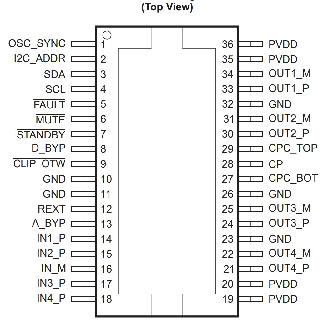
The datasheet implies that the internal DC bias point is ~3.3VDC with a common mode range of 1800mV peak to peak centered around 3.3VDC.  I interpret that to mean the common mode range spans 2.4-4.2VDC for zero differential input voltage.

Does this mean that I could force onto the IN_M common bias pin a voltage of, say, 4.0VDC and still be able to drive the class D outputs rail-to-rail without distortion?  Could I bias the IN-M pin any higher than 4V?

Assuming that I remain within the part's common mode range, is there any problem with forcing 4V onto the IN_M pin?

Alternatively, if I can get comfortable with letting the part self-bias its inputs at 3.3VDC, can I "sample" this internal bias voltage with an op amp and use that voltage to bias my external op amp?

The datasheet hints that the internal bias points are established with 85k resistors.  Thinking aloud, this means that sampling the bias voltage with an op amp exhibiting 1nA of bias current will "pull" the TAS54xx's bias point by 85 microvolts, correct?

Thanks in advance for your feedback on this topic.

Jim Olson

Indianapolis, IN US


  • Hi Jim,

    The common-mode voltage on the inputs will be the same for all the channels on the device.  The common mode voltage will vary device to device.  The input impedance has a wide tolerance also.  With the high input impedance and bias current that is pulled through this resistor will cause DC offset at the output.  You are correct in your calculation.  1nA of input bias current will cause 85uV and with 32dB of gain the output will exhibit a 3.5mV of DC offset.  1uA of bias will force a 3.5V of  DC offset! 

    You can force the input up the the maximum Vcm in the datasheet,which is 1.9Vrms, or 2.68Vpeak.  This will be the maximum allowed in each input pin above the common mode voltage.  For example.  The common mode voltage is 3.3V plus the 2.68Vpeak of signal, yields 5.98Vpeak on each input pin.  Therefore you can push it above 4.0Vdc.

    Yes, you can bias an opamp with the common mode voltage of the amplifier.  We do not provide this voltage externally, except through the input pins.  So you will need to figure how to do this in your system design.

  • Thanks for the response to my inquiry, Greg.  You are indeed the TAS54xx wizard deluxe!

    When you said in your response "We do not provide this (common mode) voltage externally, except through the input pins" you really meant that I must examine the Vcm pin with a low input bias current op amp to obtain an estimate of the part's internal common mode voltage, correct?

    And another question on an unrelated topic, if can ask without initiating another thread: 

    We will be using two TAS5424's per system, both sharing the same I2C bus.  However, because these TAS5424's are not located on the same PC board (and our products don't include AM radios where RFI is an issue) I did not plan to export an OSC_SYNC signal from first TAS5424 in the system to the second one. 

    In fact, it would be hardship in my connectorized system to export OSC waveforms between TAS5424's.  I prefer to let the two ICs internally generate their own clocks and run "unsync'ed", so to speak.

    However, if I avail myself of the chip's I2C_ADDR feature and give the two ICs different I2C bus addresses, does this mean that the TAS5424 possessing a slave I2C address has its internal oscillator entirely disabled and must receive an externally-generated OSC signal of suitable frequency and amplitude?

    If so, this probably means that I will use the I2C_ADDR pin to configure both ICs as slaves of differing I2C addresses, and provide both ICs OSC signals from local crystal oscillators.

    Thanks again for your help, Greg. 


  • Hi Jim,

    I am very happy that you have studied our device in such depth.  You are correct in that the device will automatically place itself into slave mode with a slave I2C address.  But, this slave device can be made a master by writing to Bit 6 in Register 0x0B back to Master Clock mode.

  • Greg,

    Thanks for the interesting response above to my question about use of the I2C_ADDR pin.

    Your answer suggests that I can place both of my TAS54xx devices into slave mode by driving the I2C_ADDR pin at 35%, 65%, or 100%.  In my hypothetical configuration, I would cleverly omit having an external clock waveform applied to the OSC_SYNC pin despite the chips being in slave mode.

    Then my system CPU (naturally a TI processor, right?) will issue I2C commands to the 0x0B registers to force the the internal clock circuits back to MASTER mode wherein the chips generate their own clocks.

    Am I OK so far with what you wrote?

    And so this implies that writing and reading to the I2C registers can happen successfully even if the OSC_SYNC pin is an input yet no valid external clock signal is present on OSC_SYNC  

  • Jim,

    You are correct in all your statements.

  • Greg,

    I apologize if I am monopolizing you on my silly TAS5414 questions. 

    My PCB lay-out guy just got with me and flagged a very weird issue associated with the pin-out of the 36-pin HSSOP package.  He said that documentation for this part indicates that the corner chamfer on the HSSOP-36 package is not in the traditional (upper left hand) corner.

    Furthermore, he notes that the pins are not numbered counterclock-wise around the part as traditional ICs are numbered. 

    Is this correct?

    Attached is the item of TAS5414 documentation that is turning us on our ear.

    Jim Olson
    Indianapolis, IN US
    +1.317.590.0700 cell
    Texas Instrument 36 Pin HSSOP Dimensioned Footprint.pdf

  • Hi Jim,

    Your layout guy is looking at the part upside down.  There is a round dot "lasered" near pin1 next to the exposed leadframe.  On the bottom there is a dimple in the plastic.  Since, this part is built upside down to expose the leadframe for a heatink, the marking had to be marked accordingly on the top side.

  • I reverse engineered one of the TAS5414 evaluation kits that uses the 36-pin version.  The users manual inside the eval kit contains images of the PCB copper traces.

    Based on that board lay-out, this is the correct pin-out of the 36 pin HSSOP: