This thread has been locked.

If you have a related question, please click the "Ask a related question" button in the top right corner. The newly created question will be automatically linked to this question.

TLV320AIC24K: Audio codec configuration

Part Number: TLV320AIC24K

Hi,

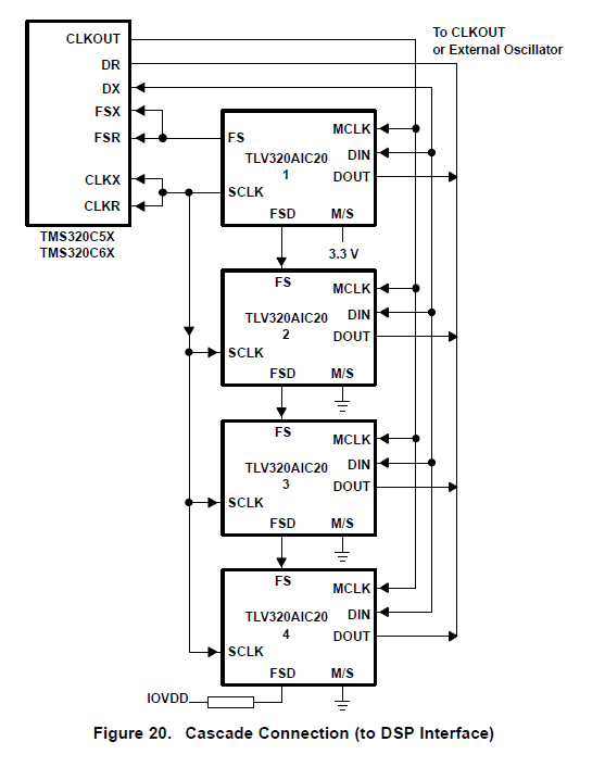
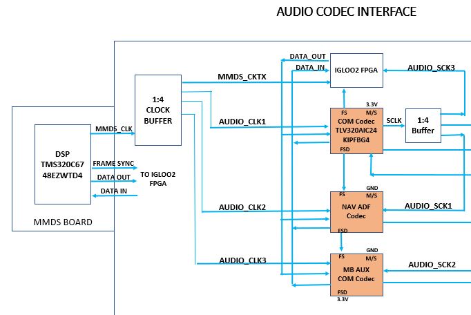
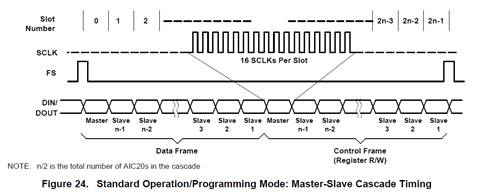
We are using three TLV320AIC24KIPFBG4 in cascaded mode in master slave configuration along with an FPGA.

The FPGA configures all three codecs and the first codec in the chain is the master.


The following is the requirement for codec configuration,

MCLK = 4.096 MHz

FS = 8 kHz

M = 4

N = 1

P = 8

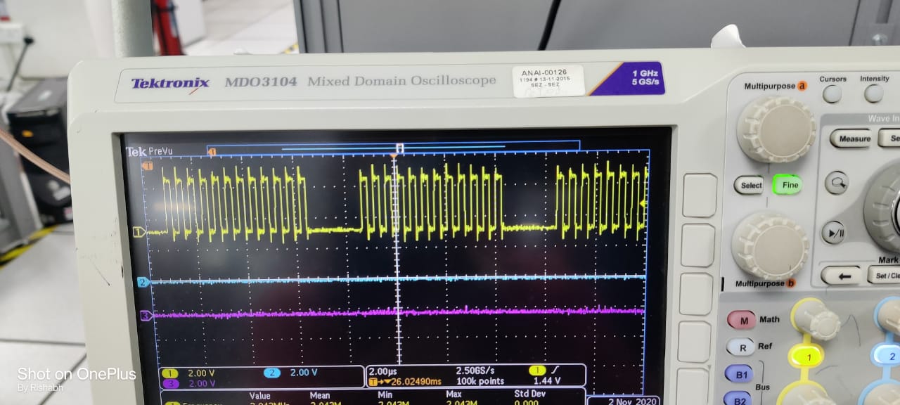
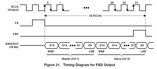
We are expecting SCLK to be 1.536 MHz based on three codec configuration.

After power up, ACD determines three codecs correctly.  But once software configures the codec, we are getting SCLK as 2.048MHz which implies four cascaded codecs.


Please confirm if our understanding on SCLK frequency is correct.

Need your urgent help in this regard.

Regards,

Archana Rao

  • Please find attached clock snapshot for reference.

    Regards,

    Archana Rao

  • Hi Archana,

    Could you share the schematic (or a diagram) of how the FPGA, primary (master) codec and the two dependent codecs are connected? Is it similar to this diagram without the last codec in the chain.

    Best Regards.

  • Hi Diljith,

    Thank you for your reply.

    Yes, it is similar to above diagram without last codec in chain.

    Please find the block diagram below for better understanding,

    Regards,

    Archana Rao

  • Not sure if you were able to see the block diagram above.

    Attaching the block diagram again.

    Re gards,

    Archana Rao

  • Hi Archana,

    The SCLK frequency should be (16 × FS × #Devices × mode). I assume the software configuration is setting the operating mode to programming mode. Please confirm. 

    For 3 AIC24s with programming mode the SCLK is expected to be 1.536 MHz. Each codec has a time slot corresponding to 64 SCLK for data transmission per sampling period.

    I understand that you are observing 2.048 MHz as the SCLK frequency. To understand this issue further please share the following with us:

    (1) Probes of the Master FS and two slave FSs along with the SCLK. There should be 64 SCLKs between the Master FS edge and the first slave FS edge. Similarly you should another 64 SCLKs between the second and third device's FS edges. 

    (2) Please comment if you are observing any performance issues on the ADC or DAC paths.

    Best Regards.

  • Hi Diljith,

    Thank you for your quick reply.

    Yes, the software configuration is setting it to programming mode.

    And as mentioned above, we are getting 64 SCLKs between two subsequent FSs.

    We are still clueless as to why we are getting 2.048MHz instead of 1.536MHz.

    We are not seeing performance issues on ADC or DAC paths.

    Need your urgent help in this regard.

    Regards,

    Archana Rao

  • HI Daljith,

    we are using following configuration,

    MCLK 4.096MHz

    We are observing SCLK is configured for Non integer division of MCLK. in current scenario.

    with M=4, N=1,P=8, SCLK=1.536MHz (non integral division of 4.096MHz) are we missing anything ?

    If SCLK is configured for integer division of MCLK we are seeing the SCLK without any gaps. (Continuous Frame syncs)

  • Hi Archana,

    Thanks for confirming that the FS signals are switching at the proper SCLK offset from the FS edge and that there is no drop in performance in any of the channels.

    These are indicative of proper functioning of the master-slave cascade.

    The M, N and P values determine the FS rate and the SCLK is automatically determined by the device depending on the number of devices in the cascade and operating mode. I do not think the higher SCLK should be a concern since there are enough SCLK cycles within the FS sampling period to transmit/receive the ADC/DAC data for all the devices in the cascade. It does not automatically mean that they system is detecting four devices in the chain. The number of devices is detected during the initialization after reset and not done through software control. And you have confirmed that ACD is giving proper device count. The reason for the higher SCLK is very likely, like you suspected, the inability to derive 1.5 MHz clock from the 4 MHz clock because of non-integer divider. I will check with the design team regarding this aspect.

    What settings did you change to get the expected SCLK? Did you have to change the M,N,P values to get a different FS?

    If you have a way to provide a 3.072 MHz MCLK with M=3, N=1 and P=8, then I would expected to see FS to 8 and SCLK to 1.536 MHz.

    Best Regards.

  • Archana,

    Figure-18 in the datasheet mentions that “SCLK may not be a uniform clock depending upon value of devnum, mode, and MNP” which is happening in this specific use-case. The design team also mentions that the non-uniform SCLK generated would be such that in one frame the average frequency of SCLK is going to be exactly same 1.536 MHz.. Therefore, we believe this is not an anomalous behavior but rather the expected behavior of the device.

    Let us know if you have any other concerns.

    Best Regards.

  • Hi Diljith,

    Thank you for your reply.

    We captured the waveforms on board today and found that we are getting 192 SCLKs between two FSs which is as per datasheet snapshot shown below.  We are getting 12 SCLKs per slot instead of 16 SCLKs.

    Can you please let us know if this behavior is expected?  Also, please let us know if we can setup a meeting to discuss with you directly for faster resolution.

    Regards,

    Archana Rao

  • Hi Archana,

    The image is not visible in the post. I will contact you directly to discuss this further.

    Best Regards.

  • For programming mode operation, the data frame and control frame timing for the cascade is expected to be as shown below.

    In the 3 device cascade, we would have

    1. Six (3 devices x 2 ch./device) 16-bit slots in the data frame resulting in 96 SCLKs
    2. Six 16-bit slots for control frame resulting in another 96 SCLKs
    3. Between two successive falling edges of FS, there would be a total of 96+96=192 SCLKs

    For average SCLK frequency is thus FS*192 = 1536 kHz.

    Now, in this case, because of the MCLK frequency and MNP values, there is no clean way to derive a continuous 1536 kHz.

    An LCM-like logic is used to arrive at the discontinuous clocks that average to 1536 kHz. So here it looks like every four SCLKs after 12 clocks are gated, resulting in an average of 3/2*2048 = 1536 kHz.

    Please note that the slot size is still fixed at 16 bits. The implication is that the slot duration varies from slot to slot. Data to/from the FPGA would have to be clocked-in/out in response to clock transition and not based on timer values. 

    Now regarding the clocking and timing of FS and FSD, the timing should be as shown below:

    Keeping in mind that SCLK could be non-uniform and that FSD is indicative of the start of the data slot for the next device, the following can be noted:

    1. FS to FSD delay could be non-uniform.
    2. FS to FSD could be different for different devices in the cascade.
    3. FSD starts after two 16-bit slots resulting in 32 SCLKs (I had mentioned 64 before, it should be 32). I had inadvertently got the control slot positions incorrect. Control slots starts after the data slots.