This thread has been locked.

If you have a related question, please click the "Ask a related question" button in the top right corner. The newly created question will be automatically linked to this question.

TPA3116D2-Q1: Request for review of circuit diagrams and defects

Part Number: TPA3116D2-Q1

Hi, Support Team

Currently during a PR event, 48 units were produced, but two units have different AUDIO LEVEL measurements.

Circuit condition: P-LIMIT MAX, 36dB GAIN

Operating conditions: 1KHz SINE WAVE PLAY, AMP input level (RMS: 42mV)

- 46 units: 1.5V output

- 2 units: 1.9V output

For the above reasons, GVDD, GAIN, and P-LIMIT are measured as follows.
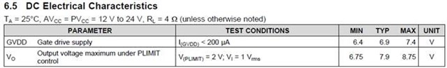
 

PR일반품

PR이상품

GVDD

6.94V

6.75V

P_LIMIT

6.94V

6.75V

GAIN

2.65V

2.59V

As above, we are examining the reason why some products have low GVDD output.

Currently, GVDD is used only for GAIN and P-LIMIT settings.

In addition, the resistance value is set according to TI's guide, but the GVDD voltage is low on some products.

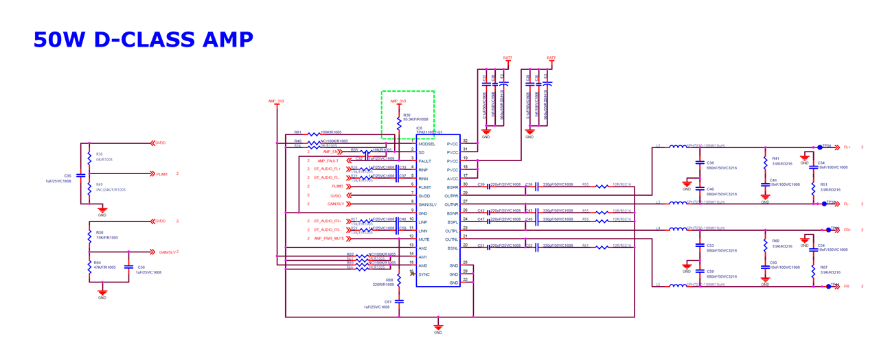
Please review the circuit configuration and capacity value by sending the circuit diagram below.

Thanks.

Regards,

MJ

  • Hi MJ,

    GVDD is generated by internal LDO, GVDD value has little variation, so datasheet shows the min and max value. From customer data, GVDD is normal.

    If PLIMIT is connected to GVDD directly, it will be no limit function.  Gain setting also has little variation, you can see the datasheet spec, Table 6.5, Gain min and max range.

    Schematic looks fine.

    Did they test output on same test point? And did they run same time before they checked output?

    I think customer test data make senses, Gain setting also has little variation.

    Regards,

    Derek 

  • Hi, Derek

    As mentioned earlier, why is GVDD low in only some parts (2pcs/48pcs)?

    I wonder why the GVDD voltage drops to 6.76V when 13.5V -> 7V -> 13.5V is performed and when MUTE is released, even if there is no

    problem because it is a product deviation and falls within the effective range.

    Also, when playing 1KHz SINE WAVE related to AUDIO output

    (Condition: 36dB GAIN, P-LIMIT MAX(0R), AMP INPUT LEVEL: 42.2mV RMS)

    When GVDD: 6.98V, AUDIO output LEVEL: 1.55V

    When GVDD: 6.76V, AUDIO output LEVEL: 1.89V

    The result is as above, but the output level differs by 340mV.

    If there is no problem with the schematic, I would like to know the reason why the GVDD power output differs even though the input power is

    the same.

    If the effective range of GVDD on the DATA SHEET is 6.4V~7.4V and everything is normal when only entering the range,

    In fact, it is expected that the AUDIO output level at 6.4V and the output level at 7.4V will show a significant difference.

    It is difficult to recognize that a situation like this is normal.

    More technically, please explain the cause of the difference in GVDD voltage and the difference in Audio Performance.

    Thanks.

    Regards,

    MJ

  • Hi MJ,

    GVDD is the power supply of internal gate driver, and GVDD is generated by internal LDO. You GVDD test result is all in spec. 

    I do not think GVDD will affect output level. But I can double confirm with designer.

    I will give you confirm information tommrrow.

    Regards,

    Derek 

  • Hi MJ,

    Confirmed with designer team, GVDD will affect Rds(on) impedance of FET. Low GVDD will make Rds(on) increasing. So the 2pcs devices with low GVDD have a little low output.

    However GVDD is generated by internal LDO, and can not adjusted. 

    Regards,

    Derek

  • Hi, Derek

    As already mentioned, the output level shows a big difference depending on the GVDD level (min~max).

    This doesn't seem to be a negligible level.

    If so, should the internally generated GVDD be seen as normal if it is between Min and Max of spec?

    The difference in GVDD value generated internally has a great influence on the performance of the product.

    Is there any way to solve this?

    Thanks.

    Regards,

    MJ

  • Hi MJ,

    If the GVDD is in datasheet spec, it must be normal value.

    GVDD can not be adjust.

    Did you test on high power output or low impedance load condition?

    GVDD influence is the Rds(on). On high power or low impedance load condition, the output current increase, it will make Rds(on) loss higher.

    Regards,

    Derek