Part Number: LMK04828
Hi sir,
In our design, we are using LMK04828 CLK Synthesizer to provide a clocks for RF-ADC & RF-DAC in RFSoC. Single LMK device with SYSREF as Feedback with Nested Dual Loopback.
LMK INPUT:
TCXO: 10MHz LVCMOS (CLKIN 0)
VCXO: 100MHz LVPECL
LMK OUTPUT:
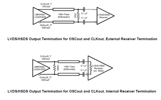
LVDS Outputs
DCLKOUTs: 150MHz
SDCLKOUTs: 3.125MHz