Part Number: CDCE72010
Other Parts Discussed in Thread: DAC3283
Hi E2E,
Our customer would like to know the proper CDCE72010 PLL configuration, please see the query as follows:
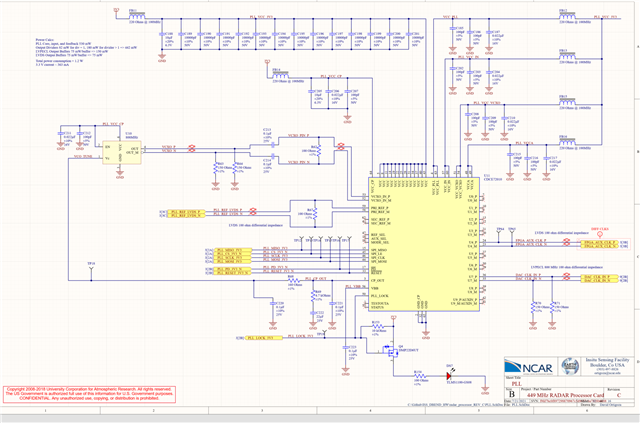
I am using a CDCE72010 PLL, and it runs very very hot on my board. I found a similar post on the forum where if you use the PLL with certain settings or in a certain configuration, it will run very hot.
This heat is causing performance issues on my board with the clocks being generated by the PLL, so I wanted to post the settings that I am using, and which clocks I need to generate, and see if there was a more efficient setup I could use.
/*
 * cdce72010_pll.c
 *
 *  Created on: Mar 30, 2018
 *      Author: alexlee
 */

#include <stdlib.h>
#include <stdio.h>
#include "xil_printf.h"
#include "sleep.h"
#include "fmc150.h"
#include "cdce72010_pll.h"

fmc_err_t pll_init()
{
	uint32_t dword;
	fmc_err_t rc;
	//Default register values
	uint32_t reg[13] = {
		0x00000000,
		0x00000001,
		0x00000002,
		0x00000003,
		0x00000004,
		0x00000005,
		0x00000006,
		0x00000007,
		0x00000008,
		0x00000009,
		0x004C013A, // reg 10 input and vxo divide counters
		0x00003EBB, // reg 11 - bit 0 and 1 primary and secondary div2 *was 3E8B now 3EBB
		0x0000000C};
	//Writeable bit mask
	uint32_t wrtbts[13] = {
		0xFFFFFFFF,
		0xFFFFFFFF,
		0xFFFFFFFF,
		0xFFFFFFFF,
		0xFFFFFFFF,
		0xFFFFFFFF,
		0xFFFFFFFF,
		0xFFFFFFFF,
		0xFFFFFFFF,
		0xFFFFFFFF,
		0xFFFFFFFF,
		0x3FFFFFFF,
		0x0000180F};

	///////////////////////////////////////////////////////////////////////////////////////////////////////////


	printf("Configure PLL for 800 MHz, with 20 MHz external reference\n");

	///////////////////////////////////////////////////////////////////////////////////////////////////////////
	//check <REVISION> field
	rc = read_fmc_reg(PLL_REG12, &dword);
	if(rc!=FMC150_ERR_OK)
		return rc;
	dword = (dword & 0x0001C000)>>14;
	if (dword!=FMC150_CLOCKTREE_PART_REV)
		return FMC150_CLOCKTREE_ERR_WRONG_PART_REV;

	///////////////////////////////////////////////////////////////////////////////////////////////////////////
	//
	//
	//INFO: The lowest 4 bits of each command word are used for addressing, so each bit shift below should be reduced
	//by 4 to compare against the chip's data sheet. For example, reg[0] += 1<<6 is actually setting the 2nd bit in reg[0]
	//not the sixth.

	///////////////////////////////////////////////////////////////////////////////////////////////////////////
	// Common register settings
	reg[0] += 0x3<<4;		//INBUFSEL (was 1 10-LVPECL now 3 11-LVDS)
	reg[0] += 1<<6;		    //PRISEL
	//reg[0] += 0<<7;		//SECSEL
	reg[0] += 0<<8;			//VCXOSEL
	reg[0] += 1<<9;			//REFSELCNTRL
	reg[0] += 0<<10;		//DELAY_PFD
	reg[0] += 0<<12;		//CP_MODE
	reg[0] += 0<<13;		//CP_DIR
	reg[0] += 0<<17;		//CP_PRE
	reg[0] += 0xF<<18;		//ICP
	reg[0] += 0<<25;		//PECL0HISWING: disabled
	reg[0] += 0x1A<<26;		//Output 0: disabled (unused)

	reg[1] += 0<<4;			//AC coupled - ACDCSEL
	reg[1] += 1<<5;			//HYSTEN
	reg[1] += 0<<6;			//TERMSEL
	reg[1] += 0<<7;			//PRIINVBB
	reg[1] += 0<<8;			//SECINVBB
	reg[1] += 0<<9;			//FAILSAFE
	reg[1] += 0<<10;		//PH1ADJC
	reg[1] += 0<<17;		//OUT1DIVRSEL
	reg[1] += 0<<24;		//EN1DIV: disabled
	reg[1] += 0<<25;		//PECL1HISWING: disabled
	reg[1] += 0x1A<<26;		//Output 1: disabled (unused)

	//********LVPECL to ADC, 80 MHz, div 10
	reg[2] += 0<<4;			//DLYM
	reg[2] += 0<<7;			//DLYN
	reg[2] += 0<<10;		//PH2ADJC
	reg[2] += 0x03<<17;		//out2divrsel: divide by 10
	reg[2] += 1<<24;		//EN2DIV: enabled
	reg[2] += 1<<25;		//PECL2HISWING: enabled
	reg[2] += 0x1A<<26;		//Output 2: LVPECL to ADC (was x20 to enable)
	//************************************

	reg[3] += 0<<4;			//DIS_FDET_REF: on
	reg[3] += 0<<6;			//BIAS_DIV01: no current reduction
	reg[3] += 0<<8;			//BIAS_DIV23: no current reduction
	reg[3] += 0<<10;		//PH3ADJC
	reg[3] += 0<<17;		//OUT3DIVRSEL
	reg[3] += 0<<24;		//EN3DIV: disabled
	reg[3] += 0<<25;		//PECL3HISWING: disabled
	reg[3] += 0x1A<<26;		//Output 3: disabled (unused)

	//********LVDS to FPGA, 400 MHz, div 2 (NOW AUX CLK)
	reg[4] += 0<<8;			//HOLDONLOR
	reg[4] += 0<<10;		//PH4ADJC
	reg[4] += 0x40<<17;		//OUT4DIVRSEL: divide by 2
	reg[4] += 1<<24;		//EN4DIV: enabled
	reg[4] += 0<<25;		//PECL4HISWING: disabled
	reg[4] += 0x3A<<26;		//Output 4: LVDS to FPGA (x1A to disable)
	//************************************

	reg[5] += 0<<4;			//BIAS_DIV45: no current reduction
	reg[5] += 0<<6;			//BIAS_DIV67: no current reduction
	reg[5] += 0<<10;		//PH5ADJC
	reg[5] += 0<<17;		//OUT5DIVRSEL
	reg[5] += 0<<24;		//EN5DIV: disabled
	reg[5] += 0<<25;		//PECL5HISWING: disabled
	reg[5] += 0x1A<<26;		//Output 5: disabled (clock out)
	//********LVPECL, 25 MHz, div 32 to DAC 			    *** new additions by dortigoza
	reg[6] += 0<<4;			//FB_FD_DESEL
	reg[6] += 0<<6;			//FBDETERM_DIV_SEL
	reg[6] += 0<<7;			//FBDETERM_DIV2_DIS
	reg[6] += 0<<8;			//FB_START_BYPASS
	reg[6] += 0<<9;			//DET_START_BYPASS
	reg[6] += 0<<10;		//PH6ADJC
	reg[6] += 0xE<<17;		//OUT6DIVRSEL					*new (x1C 32' div) xE=32 x1=8 (100mhz)
	reg[6] += 1<<24;		//EN6DIV: enabled               *new was 0
	reg[6] += 1<<25;		//PECL6HISWING: enabled         *new was 0
	reg[6] += 0x1A<<26;		//Output 6: LVPECL to DAC       *new *was x20 to enable

	//********LVPECL to DAC, 800 MHz, div 1
	reg[7] += 0<<4;			//LOCKW
	reg[7] += 3<<7;			//LOCKC
	reg[7] += 0<<9;			//ADLOCK; digital Pll lock
	reg[7] += 0<<10;		//PH7ADJC

	reg[7] += 0x20<<17;		//OUT7DIVRSEL: divide by 1
	reg[7] += 1<<24;		//EN7DIV: enabled
	reg[7] += 1<<25;		//PECL7HISWING: enabled
	reg[7] += 0x20<<26;		//Output 7: LVPECL to DAC
	//************************************

	reg[8] += 1<<4;			//VCXOBUFSEL: LVPECL
	reg[8] += 0<<6;			//VCXOACDCSEL: AC coupled termination
	reg[8] += 1<<7;			//VCXOHYSTEN: enabled
	reg[8] += 0<<8;			//VCXOTERMSEL: enabled
	reg[8] += 0<<9;			//VCXOINVBB: enabled
	reg[8] += 0<<10;		//PH8ADJC
	reg[8] += 0<<17;		//OUT8DIVRSEL
	reg[8] += 0<<24;		//EN8DIV: disabled
	reg[8] += 0<<25;		//PECL8HISWING: disabled
	reg[8] += 0x1A<<26;		//Output 8: disabled (unused)

	reg[9] += 0<<4;			//HOLDF: off
	reg[9] += 1<<6;			//HOLD#
	reg[9] += 0<<7;			//HOLDTR
	reg[9] += 0<<8;			//HOLD_CNT
	reg[9] += 0<<10;		//LOCKW
	reg[9] += 0<<12;		//NOINV_RESHOL_INT
	reg[9] += 0<<14;		//START_BYPASS
	reg[9] += 0<<15;		//INDET_BP
	reg[9] += 0<<16;		//PLL_LOCK_BP
	reg[9] += 0<<17;		//LOW_FD_FB_EN
	reg[9] += 1<<18;		//NPRESET_MDIV
	reg[9] += 0<<19;		//BIAS_DIV_FB: no current reduction
	reg[9] += 0<<21;		//BIAS_DIV89: no current reduction
	reg[9] += 0<<23;		//AUXINVBB
	reg[9] += 1<<24;		//DIS_AUX_Y9: disable AUXIN
	reg[9] += 0<<25;		//PECL9HISWING: disabled
	reg[9] += 0x1A<<26;		//Output 9: disabled (unused)


	reg[12] += 1<<11;		//PD#
	reg[12] += 1<<12;		//RESET#,HOLD#

	///////////////////////////////////////////////////////////////////////////////////////////////////////////
	// Program registers
	for (uint8_t i = 0; i < 13; i++)
	{
		rc = write_fmc_reg(CDCE72010_BASE_ADDR+4*i, reg[i]); usleep(2000); //Write
		if(rc!=FMC150_ERR_OK)
			return rc;
		rc = read_fmc_reg(CDCE72010_BASE_ADDR+4*i, &dword); //Read
		if(rc!=FMC150_ERR_OK)
			return rc;
		if( (dword&wrtbts[i]) != (reg[i]&wrtbts[i]) ) { //Check, but ignore read-only bits
			xil_printf("Clock Tree SPI Fault\n");
			return FMC150_CLOCKTREE_ERR_SPI_FAULT;
		}
	}

	//Check PLL_LOCK field (only when internal clock is chosen)
	printf("Waiting for PLL lock...");
	for (uint8_t i=0; i<10; i++)
	{
		rc = read_fmc_reg(PLL_REG12, &dword);
		if(rc!=FMC150_ERR_OK)
			return rc;
		if ((dword&0x400)!=0)
			break;
		printf(".");
		usleep(100000); //wait a while before next poll
	}
	printf("\n");
	if ((dword&0x400)==0)
	{
		printf("PLL could not lock\n");
		return FMC150_CLOCKTREE_ERR_NO_LOCK;
	}
	else
		printf("PLL locked\n");

	return FMC150_ERR_OK;

}

fmc_err_t adjust_adc_phase(uint8_t phase_setting) {
	fmc_err_t rc;
	uint32_t dword;
	uint32_t reg = 0x00000002;

	xil_printf("Setting ADC clock phase to %d\n", phase_setting);

	reg += 0<<4;			//DLYM
	reg += 0<<7;			//DLYN
	reg += phase_setting<<10;		//PH2ADJC
	reg += 0x03<<17;		//out2divrsel: divide by 10
	reg += 1<<24;		//EN2DIV: enabled
	reg += 1<<25;		//PECL2HISWING: enabled
	reg += 0x20<<26;		//Output 2: LVPECL to ADC

	rc = write_fmc_reg(CDCE72010_BASE_ADDR+4*2, reg); usleep(2000); //Write
	if(rc!=FMC150_ERR_OK)
		return rc;
	rc = read_fmc_reg(CDCE72010_BASE_ADDR+4*2, &dword); //Read
	if(rc!=FMC150_ERR_OK)
		return rc;
	if( (dword) != reg) {
		xil_printf("Clock Tree SPI Fault\n");
		return FMC150_CLOCKTREE_ERR_SPI_FAULT;
	}
	return FMC150_ERR_OK;
}
I am using an 800MHz crystal on the PLL and only need to generate 800 Mhz on channel 7 and 200 on channel 4. The input clock is 20M on the primary input
Your assistance is appreciated.
Regards,
Carlo