Hi
I have a 3.3V OSC and I want to feed the CDCVF2310PW from this OSC (at its "CLK" pin).
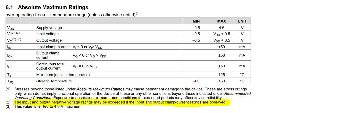
However, the target FPGAs which require the clock are working at 2.5V and therefore I want to feed the CDCVF2310PW driver from Vdd=2.5V.
My question is what is the maximum allowed voltage level at the CDCVF "CLK" pin?
In the data sheet I saw from one hand that Vih_min is 1.7V and there is no MAX but Vi (input voltage) is limited by Vdd (2.5V), so it seems as it is not proper design to feed a 3.3V clock into a 2.5V CDCVF , true?
Any suggestions how to bypass this problem (OSC Vdd requires 3.3V and FPGA requires 2.5V input clock) without changing my components?
Thanks
Amnon

-
Ask a related question
What is a related question?A related question is a question created from another question. When the related question is created, it will be automatically linked to the original question.