- Ask a related questionWhat is a related question?A related question is a question created from another question. When the related question is created, it will be automatically linked to the original question.
Hello!
I need someone to help me to check my design of the CDCLVD1208 clock buffer.
1) Input clock is 100MHz LVDS diff clock type,
2) Fanout 8 channels LVDS output clock, i use 7 channels LVDS output clock, (5 channels LVDS clock type, 2 channel LVPECL clock type)
3) My questions:
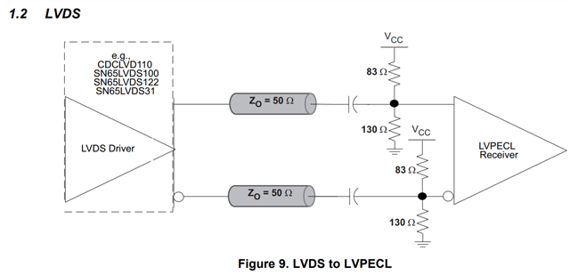
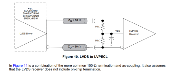
We ref TI some docs to add the pullup resisters to VCC, and add pulldown resisters to GND, convert the LVDS clock type to LVPECL type;
How can i choose the value of the pulldown and pullup resisters and the VCC ?