This thread has been locked.

If you have a related question, please click the "Ask a related question" button in the top right corner. The newly created question will be automatically linked to this question.

LMK04826: LMK04826:

Part Number: LMK04826
Other Parts Discussed in Thread: LMK04832, LMK04832EVM

Dear Sir/Madam,

We are intend to use LMK04826BISQ/NOPB device in our product, We have some following query 

1. Can we able to generate 250M Hz Clock for the FPGA.

2. Can we able to generate 50M Hz clock from this device in out of 14 Outputs. If so Please tell us the frequency stability.

regards,

sunil kumar

  • Hello Sunil,

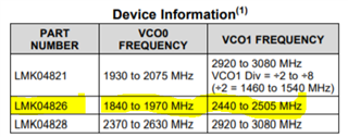
    1. Yes, the LMK04826 can output frequencies from 225 kHz to 2505 MHz.

    2. Yes, the LMK04826 can output frequencies from 225 kHz to 2505 MHz. The frequency stability can be calculated using the equation below:

    PLLx_WND_SIZE will always be set to 2 (3.7 ns window size). fPDx will be the phase detector frequency used for your PLL and can be a value between 0 to 40 MHz for PLL1 or 0 to 155 MHz for PLL2. PLLX_DLD_CNT can be a value between 1 to 16,383.

    Regards,

    Kia Rahbar

  • Hii Kia Rahbar,

    Thank you for your swift response.

    I have some query regarding the same device please help us.

    As we are generating the 8 Clocks from the  LMK04826BISQ/NOPB for other blocks in the design.

    I have listed the table of clock frequency's.  

    PLL Pins Name Pin No Clock Group Device used for the respected clock
    DCCLKOUT2 15 Clock Group 1 AFE5816ZAV
    CW clock frequency 16X  8MHz
    DCCLKOUT2* 16
    SDCCLKOUT3 13 Clock Group 1 AFE5816ZAV
    CW clock frequency 1X  2MHz
    SDCCLKOUT3* 14
    SDCCLKOUT5 22 Clock Group 2 XC7A200T-1SB484I
    FPGA 250MHz
    SDCCLKOUT5* 23
    DCCLKOUT4 24 Clock Group 2 AFE5816ZAV
    ADC  clock 5 to 80MHz
    DCCLKOUT4* 25
    SDCCLKOUT9 49 Clock Group 3 AD9102BCPZ
    DAC_1   50MHz
    SDCCLKOUT9* 50
    DCCLKOUT10 54 Clock Group 3 AD9102BCPZ
    DAC_2   50MHz
    DCCLKOUT10* 55
    OSCout 40 OSCout Group ADIN300BCPZ-R7
    Ethernet_1  25MHz
    OSCout* 41 ADIN300BCPZ-R7 Ethernet_2  25MHz
    CLKIN1_FIN_FBCLKIN 34  Clock In ( Reference clock)       125 M Hz Crystal

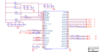
    Schematic of the Device:

    I request you please confirm us the  LMK04826BISQ/NOPB able to generate those clocks without any Interruptions during the operation.

    Looking for speedy response.

    regards,

    sunil.


  • Hi Sunil,

    LMK04826 has 7 DCLK dividers (1 to 32 div value) and one SYSREF divider (8 to 8191 div value).

    Hence, for the required clock frequencies, it can generate 250MHz output with 2500MHz VCO frequency and can generate any one of the remaining frequencies using the SYSREF divider (greater than 32) but not all at the same time.

    With the same group of channel like, DCLK0 and SDCLK1, can generate same DCLK frequencies or DCLK frequency and SYSREF at both the channels.

    Are you planning to use LMK04826 in dual PLL jitter cleaner mode or just an single PLL to generate multiple frequency?

    In dual PLL mode, OSCin required the VCXO/crystal to generate REFin for PLL2 along with external reference at CLKin1 input. In single PLL mode, external reference (125MHz) should provide at OSCin input.

    To generate all the required frequencies, I would be suggesting LMK04832, which is pin compatible with LMK0482x devices and have DCLK dividers (1 to 1023 div value) and SYSREF divider (8 to 8191 div value). 2MHz clock out can be generate using the SYSREF dividers.

    Hope, it clarifies your queries.

    Please let us know, if you need further assistance on it.

    Thanks!

    Regards,
    Ajeet Pal

  • Hii Ajeet Pal,

    Thank you for the replay, We are New to the clock Jitter Topic So please help us to clarify below query.

    1. LMK04826 has 7 DCLK and 7 SDCLK.

    As we need 7 different clock frequencies in our design. i think with this device we can generate without any issues using 7 DCLK channels. Please confirm us our understanding is correct or wrong.

    2. With respect to the above Point we need 8MHz, 250MHz, 80MHz, 50MHz, 50MHz As a Differential Clock. Can we able to generate these frequencies using   DCLKout0, DCLKout2, DCLKout4,DCLKout6, DCLKout12, DCLKout10. Please Conform. 

    Note: If some error in the above configuration please help us with the detailed description.

    3. We need two clock outputs in LVDS Format with the frequency about 50MHz in two channel.

    As with reference  to the LMK04826 Datasheet 9.1.9 Clock Distribution section.  OSCout may be a buffered version of OSCin, DCLKout6, DCLKout8, or SYSREF. We are planning to use OSCout  (Pin No. 40 and 41)as a LVDS Pair.

    We assume that DCLKout6 buffer version  is OSCout. So we can make modification in Program. Please confirm this Part.

    4. Please tell us what is the Minimum Clock frequency we can generate in DCLK output channels.

    Looking for speedy response.

    regards,

    Sunil

  • Hi Sunil,

    1. LMK04826 has 7 DCLK and 7 SDCLK.

    As we need 7 different clock frequencies in our design. i think with this device we can generate without any issues using 7 DCLK channels. Please confirm us our understanding is correct or wrong.

    Yes, LMK04826 can generate 7 DCLK frequencies with the maximum division value 32.

    2. With respect to the above Point we need 8MHz, 250MHz, 80MHz, 50MHz, 50MHz As a Differential Clock. Can we able to generate these frequencies using   DCLKout0, DCLKout2, DCLKout4,DCLKout6, DCLKout12, DCLKout10. Please Conform. 

    Note: If some error in the above configuration please help us with the detailed description.

    As mentioned earlier, to have 250MHz clock out from LMK04826, required VCO will be 2500MHz. Hence it can't generate other required frequencies, 80MHz (div needed - 31.25), 50MHz (div needed - 50), 8MHz (div needed - 312.5) with integer dividers up to 32 value, except with the SYSREF divider.

    3. We need two clock outputs in LVDS Format with the frequency about 50MHz in two channel.

    As with reference  to the LMK04826 Datasheet 9.1.9 Clock Distribution section.  OSCout may be a buffered version of OSCin, DCLKout6, DCLKout8, or SYSREF. We are planning to use OSCout  (Pin No. 40 and 41)as a LVDS Pair.

    We assume that DCLKout6 buffer version  is OSCout. So we can make modification in Program. Please confirm this Part.

    If LMK04826 is not operating in zero-delay mode, then OSCout can be set with the DCLK6, DCLK8 or SYSREF signal using the Feedback mux and can generate output at OSCout pins in LVDS format or other too. DCLK6 can be set to OSCout using feedback mux with required frequency.

    4. Please tell us what is the Minimum Clock frequency we can generate in DCLK output channels.

    With the minimum internal VCO frequency (1840MHz) and maximum DCLK channel divider (32), minimum clock out frequency would be 57.5MHz at DCLK channels.

    Thanks!

    Regards,
    Ajeet Pal

  • Dear Ajeet Pal,

    Thank you so much for you help.

    As we need all different frequencies in 5 different channel. As you mentioned we canot be able to generate those frequencies using  LMK04826 Device. As you mentioned in earlier email we are planning to switch  LMK04832 device.

    1. As we understood from the datasheet of LMK04832 we can divide the VCO Clock (1 to 1023 div value). Could you please confirm that our understanding is correct. and we can able to generated this frequencies in dedicated channel   8MHz, 250MHz, 80MHz, 50MHz, 50MHz.

    2. we need two 50 MHz clock source to drive two blocks in our design. The output clock source should be single ended LVCMOS Clock. Could you please help us to this issue how we can generate using LMK04832 Device.

    3. Please give the clarity of 2x LVCMOS. (Please explain why it is 2x). if we want to use LVCMOS Clock source from one of the LVCOMS Generated channel.

    As there is two outputs in  LMK04832 channel how to use for this single ended clock source devices.

    4. As we need to provide a reference clock source to LMK04832. we are planning to use external crystal of 122MHz. Please suggest us  where to connect the crystal Because we could see we there are three clock inputs in the data sheet. 

    Note: Expecting quick response as we are in critical stage of design 

    regards,

    Sunil

  • Hi Sunil,

    1. As we understood from the datasheet of LMK04832 we can divide the VCO Clock (1 to 1023 div value). Could you please confirm that our understanding is correct. and we can able to generated this frequencies in dedicated channel   8MHz, 250MHz, 80MHz, 50MHz, 50MHz.

    That's correct. LMK04832 supports DCLK clock divider values from 1 to 1023. To generate all required frequencies, proper frequency planning is needed, including its reference input. Like with the 125MHz reference input and considering 250MHz critical required frequency, then VCO frequency can be 3000MHz and it can generate all required frequencies except 80MHz, cause its not integer divided value from 3000MHz. Hence need to change the 80MHz clock frequency. Similarly, if 80MHz is critical clock frequency, then can select the VCO frequency 3200MHz, which can generate all required frequencies with 100MHz reference input except 250MHz.

    2. we need two 50 MHz clock source to drive two blocks in our design. The output clock source should be single ended LVCMOS Clock. Could you please help us to this issue how we can generate using LMK04832 Device.

    LMK04832 supports LVCMOS output at 9 clock out channels and can generate 2 numbers 50MHz single ended LVCMOS signals from single channel.

    3. Please give the clarity of 2x LVCMOS. (Please explain why it is 2x). if we want to use LVCMOS Clock source from one of the LVCOMS Generated channel.

    As there is two outputs in  LMK04832 channel how to use for this single ended clock source devices.

    Each differential pins can be set for LVCMOS outputs with Norm / INV (in-phase / 180deg out of phase). That's 2x represents the number of LVCMOS output from each channel. Hence, total you can generate 18 LVCMOS outputs from 9 channels.

    4. As we need to provide a reference clock source to LMK04832. we are planning to use external crystal of 122MHz. Please suggest us  where to connect the crystal Because we could see we there are three clock inputs in the data sheet. 

    Bit confused with your reference clock frequency, is it 125MHz (in previous comment) or 122MHz? Anyways that's come under your frequency planning and need to choose carefully. 

    LMK04832 has the flexibility to provide the reference from any of the inputs. If single PLL is needed (PLL2), you can connect at OSCin pins. For dual PLL mode also, you can keep at OSCin pins and can provide other reference at CLKin0/CLKin1.

    Thanks!

    Regards,

    Ajeet Pal

  • Hii Ajeet Pal,

    Thank you so much for your Response!!!!,

    We have got a fair clarity on this LMK04832 device. As we are Moving to the Layout Design, Could you please suggest us what is the Impedance need to be followed on Differential Pair Clocks and a LVCMOS Clock. 

    I request you to please suggest us Min and max Trace length in the PCB To be followed on clock signals. 

    As we are using single ended LVCMOS Clock from the Differential Pair. How do we configure the left out pin in the Respected channel. Do we need to leave Float or Pulled to High or Pulled to ground. 

    As for your Kind Information we are Planning to use 125M Hz Crystal for the reference clock.

    regards,

    sunil Kumar

  • Hi Sunil,

    We have got a fair clarity on this LMK04832 device. As we are Moving to the Layout Design, Could you please suggest us what is the Impedance need to be followed on Differential Pair Clocks and a LVCMOS Clock. 

    I request you to please suggest us Min and max Trace length in the PCB To be followed on clock signals. 

    Below thread provides the LMK04832EVM design files FYR, which gives the details of device layout constraints and trace details. Device output differential pairs run with 100ohm impedance and for LVCMOS trace will run in 50ohm single ended transmission line. Follow the layout guidelines mentioned in datasheet.

    https://e2e.ti.com/support/clock-timing-group/clock-and-timing/f/clock-timing-forum/963976/lmk04832evm-schematic-layout-files

    As we are using single ended LVCMOS Clock from the Differential Pair. How do we configure the left out pin in the Respected channel. Do we need to leave Float or Pulled to High or Pulled to ground. 

    For LVCMOS single ended lines are routed 50ohms and unused pins diverse from differential lines and unused can be leaving the output floating close to the IC. Alternatively, place a 50-Ω termination at the end of an unused trace, if routed differentially from device and split to 50 ohm after that.

    As for your Kind Information we are Planning to use 125M Hz Crystal for the reference clock.

    Frequency planning is needed based on reference clock frequency and required output frequencies,

    Thanks!

    Regards,

    Ajeet Pal