This thread has been locked.

If you have a related question, please click the "Ask a related question" button in the top right corner. The newly created question will be automatically linked to this question.

LMK04832: Clkin0 as SYNC input.

Part Number: LMK04832
Other Parts Discussed in Thread: LMX2820, LMK04828

Hi Team,

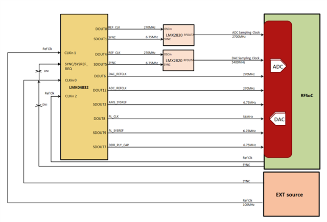
we are using LMK04832 in our design and i have few quries regarding Clkin0 as SYNC input.

If we are using Clkin0 as SYNC input, whether it should be a single ended or differential.?

If it can be of both type, How it should be connected to LMK04832 if it is single ended or if it is diiferential? 

Suggest me if any ac coupling or terminations required for both the cases.

--

Thanks in Advance,

Kiran

  • Hi Kiran,

    SYNC input at CLKin0 provide the precise timing for synchronization and required DC coupled differential input.

    Regards,

    Ajeet Pal

  • Hi Ajeet,

    Thank you for the reply,

    In our design the SYNC will be single ended signal provided from external source, May i know how to connect this single ended signal as differential to LMK04832?

    May I request you to provide feedback on few more questions mention below?

    We are using LMK04832 and LMX2820 in our design for ADC and DAC sampling clock generations. our clock architecture is as shown below.

    LMK input:

    LMK04832 default has 100MHz input to clockin1 provided from external source, 100 MHz VCXO input to OSCin and sync signal input to Clockin0. (Optional Ref clock and sync is provided to Clockin2 and SYNC/SYSREF_REQ pin).

    LMK outputs:

    DCLKOUT0 : 270MHz( input to first LMX2820)

    SDCLKOUT1: sync to first LMX2820

    DCLKOUT4: 270MHz( input to second LMX2820)

    SDCLKOUT5: sync to second LMX2820

    SDCLKOUT3: 6.75MHz AMS_SYSREF

    DCLKOUT6:  270MHz DAC_REFCLK

    SDCLKOUT7:  6.75Mhz DDR_PLY_CAP

    DCLKOUT8: 54MHz PL_CLK

    SDCLKOUT9: 6.75MHz PL_SYSREF

    DCLKOUT12: 270Mhz ADC_REFCLK

     AMS_SYSREF, PL_CLK, PL_SYSREF requires synchronization and alligned to each other.

    a. We are using LMK04832 in dual loop mode and in order to generate required output, VCO1 of PLL2 is used at 3240MHz frequency. Since datasheet specifies the max frequency of VC01 is 3255MHz, will be there any performance issue of VC01 since we are using at the upper edge of VC01?

    PFA the Ticspro file FYR.

    Please verify the Ticspro configurations for our requirements and provide the suggestions.

    b. Since SYNC is single ended, May i know how to connect this single ended signal as differential to LMK04832 clockin0. Can you please verify with our schematics.

    c. Regarding clockout terminations as per LMK04828 datasheet, ( since LMK04832 and LMK042828 are pin to pin compatible, we reffered LMK04828 for output terminations), clock out signals which doesnt have internal termination at receiver, should be terminated as 

    Our DDR_PLY_CAP, PL_CLOCK, PL_SYSREF doesnt have internal termination and requires 100ohm external termination usually after coupling capacitor towards the load pin, but LMK04828 datasheet recommends to use 100E termination before coupling capacitor towards LMK. which one to follow? in our design we have provied optional 100E termination after coupling capacitor which will be DNI. Can you confirm whether that can be removed? (refer pg5 of attached schematic).

    D. PFA the schematics and verify the LMK, LMX designs with respect to clock inputs , outputs and its terminations, loop filter values and power section design powering LMK and LMX and provide the feedback.

    MS_TI_SCH_Review.pdf

    WBRFU_LMX_270MHz_5400MHz.tcs

    WBRFU_LMK_270MHz_6M75Hz.tcs

    --

    Thanks in Advance,

    Kiran

  • Hi Kiran,

    Since you have single-ended SYNC, I suggest put CLKin0 as MOS input.

    We test VCO frequency coverage in production, so there is no issue even if you operate it at the min./max. frequency.

    You have a 27MHz domain system, I suggest change the VCXO to 108MHz or 135MHz so that you can maximize PLL2 fpd. With a 100MHz VCXO, the highest fpd you can use is just 20MHz, output phase noise from PLL2 is not going to be excellent. 

    the LMX tcs file is same as the LMK tcs file, please send us the correct LMX tcs file.

    Figure 30 is correct. LVDS is a current source, the current flowing through the resistor will therefore create a voltage across the resistor. If the receiver is a standard LVDS receiver, then the DC-blocking capacitors are not needed. If the receiver requires AC-coupling, then Figure 30 is exactly what you need.

    I recommend use the OSCout from LMK PLL1 as the reference clock to the LMX devices because the noise from PLL2 will be carried forward to LMX output. If OSCout is not available due to CLKin2, then use a clock buffer to fanout the VCXO signal.

    schematic looks good.

  • Hi Noel,

    Sorry for the wrong LMX tcs file, PFA the correct LMX tcs file.

    7080.WBRFU_LMX_270MHz_5400MHz.tcs

    You have a 27MHz domain system, I suggest change the VCXO to 108MHz or 135MHz so that you can maximize PLL2 fpd. With a 100MHz VCXO, the highest fpd you can use is just 20MHz, output phase noise from PLL2 is not going to be excellent.

    Regarding VCXO frequency, As per mistral's design VCXO is 100MHz, that would reduce the  PLL1 N / R ratio R =1,  But PLL2 N / R ratio will not reduce such that R = 1. However,if the VCXO is 108MHz or 135MHz, PLL2 N / R ratio will reduce such that R = 1 but not the PLL1. 

    Is it always required to have N / R ratio of PLL1 and PLL2 such that R reduce to 1 or use of SYNC signal is enough for synchronization of clock outputs?

    I recommend use the OSCout from LMK PLL1 as the reference clock to the LMX devices because the noise from PLL2 will be carried forward to LMX output. If OSCout is not available due to CLKin2, then use a clock buffer to fanout the VCXO signal.

    LMX outputs are used to generate the sampling clock and  are required to be synchronized with LMK outputs AMS_SYSREF, PL_CLK, PL_SYSREF and phase alligned to each other.

    We would also require multi clock synchronization using external SYNC singal. Can we achieve the required synchronization from your recommendation?

    Regarding VCXO selection, VCXO used in LMK04832 EVM is LVPECL output, but the one we used in our design is LVCMOS. Will there be any performance issue due to change in output type?

    --

    Thanks in Advance,

    Kiran

  • Hi Kiran,

    the loop bandwidth of PLL1 is going to be very small and it does not require a high fpd. So if you use 108MHz VCXO, PLL1 fpd = 1MHz, which is same as if you are using a 100MHz VCXO. PLL2 requires higher fpd in order to reduce PLL noise and make loop bandwidth wider. if you want as low jitter as possible, the VCO frequency should be an integer multiple of VCXO frequency. As long as the phase noise is identical, there will be no performance difference between LVPECL and CMOS VCXO at this frequency. The SYNC signal is use to phase align all the clock outputs, it does not have to be very low noise. 

    CLKout and OSCout will have some deterministic delay (a few nano-second) which should not post an issue considering that your SYSREF frequency is low. Otherwise, you can put the LMK device in 0-Delay Dual Loop Mode such that the clock outputs will be phase aligned with OSCout. 

    As for LMX configuration, you can make fpd = 270MHz in order to get lower in-band noise.

  • Hi Noel,

    You have a 27MHz domain system, I suggest change the VCXO to 108MHz or 135MHz so that you can maximize PLL2 fpd. With a 100MHz VCXO, the highest fpd you can use is just 20MHz, output phase noise from PLL2 is not going to be excellent.

    I am not abe to find good VCXO of 108MHz or 135MHz with low phase noise and Phase jitter. Do you have any recommended part numbers for this VCXO frequencies?  Your suggestions will we helpfull.

    --

    Thanks in Advance

    Kiran

  • Hi Kiran,

    For the specific frequency VCXO, you can reach out to the different vendors who can suggest an specific parts. The major vendor list includes Crystek crystals, Skyworks, vectron etc.. for VCXO. For your required frequencies, you can consider the 90MHz VCXO also.

    Regards,

    Ajeet Pal

  • Hi Ajeet

    I reached out few vendors and they are yet to come back to my query. Few part which i gone through do not have low phase jitter as in the parts used in LMK04832 and CLK104 board of ZCU208 EVM ( typical phase jitters of parts used in LMK04832 and CLK104 board are within 80 femto seconds while the part for 90MHz, 108MHz, 135MHz are in range of 0.2 ps to 1 ps ). 

    Is it good to use 120MHz VCXO with N prescaler of PLL2 VCO as 3 and R divider as 9 so that my PLL2 fpd will be 120MHz. 

    --

    Thanks in Advance

    Kiran

  • Hi Kiran,

    Yes, you can use the 120MHz VCXO with 3240MHz VCO frequency and PLL will lock with above shown N-prescaler and N-divider values. R-divider value can keep 1. 

    Regards,

    Ajeet Pal