HI team
Section 8.1.3.2 and 8.4.2.1 states that OSCout can be provided before programming LMK04832-SP. If I provide a LVDS osc to OSCin, what will be the default OSCout buffer type?
Also, In section 8.2 Functional Diagram, it indicates that it is SPI selectable. By default it is OSCin or do I need to program that?
Also, if LMK04832-SP is powered up...what is the time from power up and the output of OSCout?
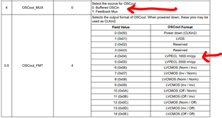
8.1.3.2 External VCXO for PLL1 When PLL1 is used, an external VCXO is required. The close-in noise performance of this VCXO is critcal for good jitter cleaning performance. The LMK04832-SP also provides OSCout, which by power-on default is a buffered copy of the PLL1 feedback and PLL2 reference input at OSCin. This reference input is typically a low noise VCXO or XO. This output can be used to clock external devices such as microcontrollers, FPGAs, CPLDs, and so forth, before the LMK04832-SP is programmed. • The OSCout buffer output type is programmable to LVDS, LVPECL, or LVCMOS. • The VCXO buffered output can be synchronized to the VCO clock distribution outputs by using Cascaded 0- Delay Mode.
8.4.2.1 PLL2 Single Loop
Best Regards,
William