Part Number: CDCE6214
Hello TI,
After spending too many hours attempting to decipher the cdce6214 datasheet (snas811), please assist with the following:
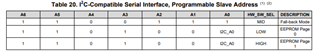
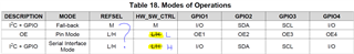
1) Apparently, HW_SW_CTRL decides whether the device enters Pin Mode or not. If so, why does snas811 Table 18 have "L/H" for this entry? Should this not be "L" ? Should snas811 Table 18 not perhaps look more like this:
Should the HW_SW_CTRL column not perhaps move left in this Table to indicate its role in mode selection?
2) Is Fall-back mode determined only by HW_SW_CTRL (as Table 20 might imply), or by the combination of HW_SW_CTRL and REFSEL (both "M", according to Table 18)?
3) Does REFSEL = M have any other role other than possibly in conjunction with HW_SW_CTRL = M? With other words, what is the effect of the following:
HW_SW_CTRL = L and REFSEL = M
HW_SW_CTRL = H and REFSEL = M
HW_SW_CTRL = M and REFSEL = L
HW_SW_CTRL = M and REFSEL = H
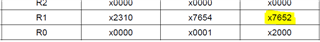
4) snau247b has
0x1000 as default for register R0 and
0xA020 as default for R15 and
0x0000 as default for R16,
for example (there are others). However, snas811 has:
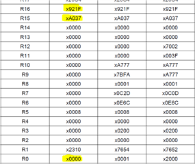
Is there a discrepancy, perhaps? If so, which is correct?
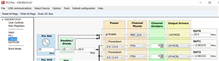
5) OUT0 can seemingly be sourced from ahead of the "x2" doubler and "R div" divider blocks, but this is not apparent in snas811 Figure 23. Would it be possible to show this option?
Thanks!