This thread has been locked.

If you have a related question, please click the "Ask a related question" button in the top right corner. The newly created question will be automatically linked to this question.

LMK04828: LMK04828 tecnology support for TICS pro

Part Number: LMK04828

Hi,

We use the LMK04828 in our new project and we have the below issue for this device:

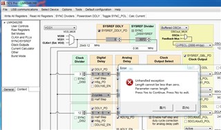
1. We use the TICS pro to set the LMK04828, and the error as below:

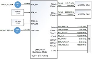
2. Please advise how to set below CLK, thanks.

  • Zhang,

    It's not clear to me what you've done to generate this exception. Was there a specific control you interacted with to trigger this error? Can you describe the steps you took to generate this error?

    Can you navigate to C:\Program Files (x86)\Texas Instruments\TICS Pro, and share the ErrorLog00.txt file and log00.txt/log01.txt files if present?

    Regards,

    Derek Payne

  • Hi Derek,

    Attach for your evaluating, thanks.

    TICS Pro.exe Warning: 0 : 04/08/2022 10:52:34
    Unhandled exception
    长度不能小于 0。
    参数名: length
    ----------------------------------
    
    Welcome to TICS Pro. Version -> 1.7.4.1, 10-Feb-22
    Loading Device LMK04828B...
    Detected 0 USB2ANY interfaces
    Completed loading Device LMK04828B. Version = 2019-06-12, v4.0.0, scripts=fa67100541
    

  • Zhang,

    I've identified three places in the code that could be raising the error you describe:

    1. Attempting to load a configuration
    2. Attempting to save a configuration
    3. Attempting to open the Communication Setup dialog from the "USB Communications -> Interface" menu.

    Which of these were you attempting?

    ---

    I've reviewed your configuration request, and I have a few comments before we proceed:

    • You will have trouble getting 160MHz VCXO to generate the frequencies you want. I recommend 122.88MHz VCXO, since this will be much easier to generate the 2457.6MHz VCO frequency in PLL2.
    • Using a 156.25MHz clock on the CLKin2 path in addition to the 10MHz references and the 122.88MHz VCXO reduces the best case PFD frequency to 10kHz at PLL1; this isn't necessarily an issue for loop stability or phase noise, but it will take a long time for PLL1 to lock.
    • I see you have some outputs that are using the 7.68MHz clock as SYNC or SYSREF. Are you planning to use this as a continuous clock in any places? Note that there is only one SYSREF distribution mechanism, which means all outputs using the SYSREF divider must be all pulsed or all continuous.
    • What are the input and output formats that should be used (e.g. LVPECL, LVDS)?

    Regards,

    Derek Payne

  • Hi Derek,

    The error is the load a configruration, and we choose the File ----> load ----- LMK04828, and the error show as the attach;

    For the section 2, we will test first and many thanks for your kindly support

  • Hi Derek,

    For the section 2, pleaes refe to below reply:

    • You will have trouble getting 160MHz VCXO to generate the frequencies you want. I recommend 122.88MHz VCXO, since this will be much easier to generate the 2457.6MHz VCO frequency in PLL2.
    • -------------[Dongliang] OK, we will update the VCXO to 122.99MHz;
    • Using a 156.25MHz clock on the CLKin2 path in addition to the 10MHz references and the 122.88MHz VCXO reduces the best case PFD frequency to 10kHz at PLL1; this isn't necessarily an issue for loop stability or phase noise, but it will take a long time for PLL1 to lock.
    • -------------[Dongliang] 156.25MHz is the SFP clock recover, and FPGA will frequency division and how to set the frequency?
    • I see you have some outputs that are using the 7.68MHz clock as SYNC or SYSREF. Are you planning to use this as a continuous clock in any places? Note that there is only one SYSREF distribution mechanism, which means all outputs using the SYSREF divider must be all pulsed or all continuous.
    • -------------[Dongliang] Yes, all the SYSREF divider are continuous;
    • What are the input and output formats that should be used (e.g. LVPECL, LVDS)?
    • -------------[Dongliang] The output signle of  DOUT3、DOUT6、DOUT12 are LVPECL; The output of DOUT7、DOUT8、DOUT9 areLVDS; Input of 10MHz is 3.3V, the schematic as attahc, thanks.
    • 8228.LMK04828 SCH.pdf
  • Hi  Derek,

    Is there any comment, thanks.