- Ask a related questionWhat is a related question?A related question is a question created from another question. When the related question is created, it will be automatically linked to the original question.
This thread has been locked.
If you have a related question, please click the "Ask a related question" button in the top right corner. The newly created question will be automatically linked to this question.
I am using two-channel clock SDCLKout7 and SDCLKout11 to output 2GHz clock. I need to synchronize the two outputs according to the description in the manual, as shown below:
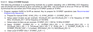
What do I need to do to fulfill my requirements? Does the manual describe how to modify the corresponding value during the configuration from 0x000 to 0x1FFF (my configuration sequence is generated by the software), or do I need to configure the data after or before the configuration? I'm sorry that I didn't fully understand the meaning of the example. I would appreciate it if you could help me elaborate
Hi,
For the sync output, you need to follow the SYNC procedure mentioned below:
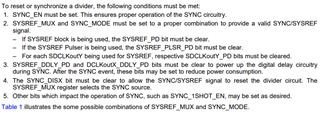
If you wants to operate at 2GHz at SDCLKout7 and SDCLKout11, this frequency will be directly from VCO (without channel dividers) and should be synchronized to each other. It needs to be configured SDCLKout7 and SDCLKout11 with device clock out.
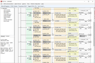
You can use the TICS Pro tool to configure the device.
Thanks!
Regards,
Ajeet Pal
Hi,
Thank you for your reply and answer above, but I want to know at which stage the status bits I need to modify are carried out. It seems that the sequence generated by the software does not contain the status bits mentioned above. Since I am not a hardware engineer, I do not quite understand the use of your software. I hope you can give me more information to answer my doubts.
Thanks!
Regards,
ShuJie
Hi Ajeet,
I want to add some info here for this case, actually the key question is that:
How to complete the following specific register in the FPGA code? Since the register 0x0000 to 0x1fff is generated by our tics or codeloader directly. Should we place the following setup before generated register loading or after the register loading.
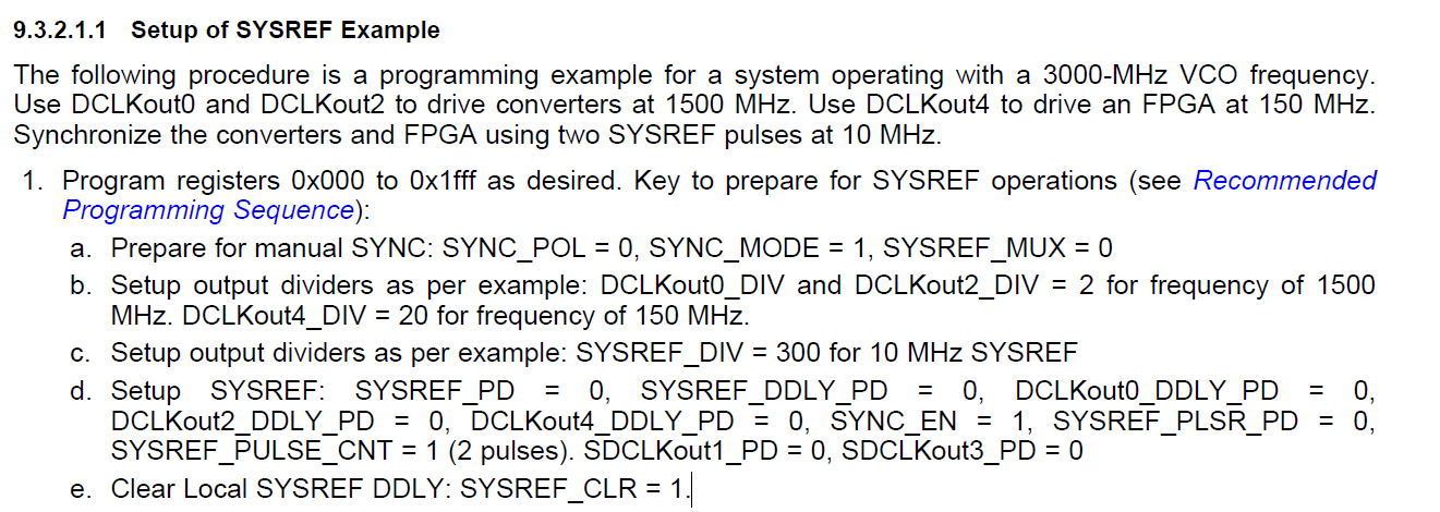
And how to change the specific register status in their code, such as SYSREF_CLR.
Thanks
Best regards
Mia Ma
Hi Mia, ShuJie,
For the programming, you should first program all registers as mentioned in "Recommended Programming Sequence" section then for SYNC and /or SYSREF operation, you can go required registers update mentioned for each example.
For individual bits update, need to write particular address register with the bit update, like for SYSREF_CLR, you need to write x143 register with [7] bit update.
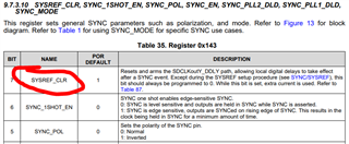
I hope, it clarifies your question.
Thanks!
Regards,
Ajeet Pal
As I understand it, I set 0x140 to 0x00 and 0x143 to 0x91, based on the following picture:
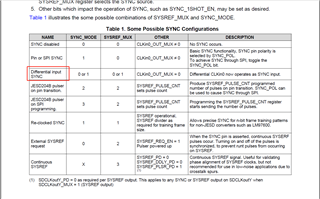
My combination is Differential input SYNC, so I didn't care about SYSREF_MUX and SYNC_MODE status, but that didn't work out as I expected, did I have a configuration error?
According to the screenshot below:

I checked the registers that need to be configured one by one, except the above two, the others have been configured to the expected values when the software was generated, so I didn't modify them. In addition, since I need to synchronize the same clock frequency, I'm too sure how many bits SYSREF_PULSE_CNT need to be configured, please give me some technical guidance.
My register sequence is as follows:
R0 (INIT) 0x000090
R0 0x000010
R2 0x000200
R256 0x010000
R257 0x010155
R259 0x010345
R260 0x010402
R261 0x010500
R262 0x0106F0
R263 0x010733
R264 0x010810
R265 0x010955
R267 0x010B45
R268 0x010C02
R269 0x010D10
R270 0x010EF0
R271 0x010F01
R272 0x01100A
R273 0x011155
R275 0x011347
R276 0x011402
R277 0x011500
R278 0x0116F0
R279 0x011701
R280 0x011801
R281 0x011955
R283 0x011B45
R284 0x011C22
R285 0x011D06
R286 0x011EF0
R287 0x011F16
R288 0x012008
R289 0x012155
R291 0x012300
R292 0x012402
R293 0x012500
R294 0x0126F8
R295 0x012700
R296 0x012801
R297 0x012955
R299 0x012B45
R300 0x012C22
R301 0x012D00
R302 0x012EF0
R303 0x012F16
R304 0x013019
R305 0x013155
R307 0x013345
R308 0x013402
R309 0x013500
R310 0x0136F0
R311 0x013733
R312 0x013805
R313 0x013905
R314 0x013A1F
R315 0x013BFF
R316 0x013C00
R317 0x013D08
R318 0x013E03
R319 0x013F00
R320 0x01400A
R321 0x014100
R322 0x014200
R323 0x014310
R324 0x01447F
R325 0x01457F
R326 0x014618
R327 0x014718
R328 0x014802
R329 0x014942
R330 0x014A02
R331 0x014B16
R332 0x014C00
R333 0x014D00
R334 0x014EC0
R335 0x014F7F
R336 0x015003
R337 0x015102
R338 0x015200
R339 0x015300
R340 0x015478
R341 0x015500
R342 0x015678
R343 0x015700
R344 0x015896
R345 0x015900
R346 0x015A78
R347 0x015BD4
R348 0x015C20
R349 0x015D00
R350 0x015E00
R351 0x015F0B
R352 0x016000
R353 0x016101
R354 0x016200
R355 0x016300
R356 0x016400
R357 0x016519
R372 0x017405
R380 0x017C15
R381 0x017D33
R358 0x016600
R359 0x016700
R360 0x016819
R361 0x016951
R362 0x016A20
R363 0x016B00
R364 0x016C00
R365 0x016D00
R366 0x016E13
R371 0x017300
R8189 0x1FFD00
R8190 0x1FFE00
R8191 0x1FFF53
Thanks!
Regards,
ShuJie
Hi ShuJie,
For differential SYNC input at CLKin0, you doesn't necessary bother about SYNC_MODE and SYSREF_MUX settings. CLKin0 direct feed to SYSREF_CLKin0_MUX and set for "From CLKin0" and can synchronize the device with this. To reset the required channel dividers set SYNC_DISx and SYNC_DISSYSREF bits to 0 and input the SYNC. Once dividers are reset, change SYNC_DISx and SYNC_DISSYSREF bits to 1.
Then if you wants to set the SYSREF outputs in pulsar mode, follow the below sequence:
0x139 --> 0x02
0x143 --> 0x13
For sending the SYSREF pulses through SPI at desired SDCLKoutx channel, write 0x13E --> 0x03.
Hope, it clarifies your queries.
Thanks!
Regards,
Ajeet Pal