This thread has been locked.

If you have a related question, please click the "Ask a related question" button in the top right corner. The newly created question will be automatically linked to this question.

TLC555: TLC555CD

Part Number: TLC555

Hi,

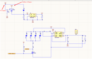
I designed  a latch circuit using TLC555CD. I am facing an issue that if i leave circuit OFF then battery discharge. It is LED ON/OFF circuit. Can anyone help me to find the issue or suggest me some alternative for a latch circuit. The latch circuit must be trigger with a vibration switch.
Plz see the attached schematic.
Thanks
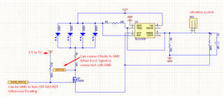


LED

Vibration Switch

  • Hello,

    I do not see a problem in your circuit that will consume large amounts of current in the off state. In order to be "OFF" the output of the 555 must be high. This is what you mean by "leaving the circuit OFF" correct? If this is the case there will be current consumption to keep the 555 working. This will cause the battery to discharge. I am assuming 3.3V is the battery.

    If I may, why are you using the NFET? Is there a specific reason for this? Must your latching circuit use a 555 timer?

    Regards,

    Cas

  • Hi 
    Thanks for your response.

    Regarding 555 timer, No it is not must to use 555 timer. The important component is vibration switch. If you can help me to define an easy latch circuit. It would be great.

    I am using NFET to control LED through external signals.
    This circuit has two functions.

    1. Control through vibration switch
    2. Control through external signals

    When no external signal(Dock signal and Switch) are available then LED will be ON/OFF using vibration switch but when external signal will apply then i want to completely eliminate the use of latch circuit and complete control shift to the external signals.

    The switch Node basically connect ground directly at that node point through external connection and dock signal also provide GND signal to turn OFF Mosfet.

    YES 3.3V is the regulated voltage from the battery while VIN is directly connected with battery.

    One more thing, I am using a single cell lipo battery with 100mAh rating.

    I also used a linear regulator to regulate lipo voltages which is also another issue in my design but it is for another day.

    Let me know if you have any further questions.

  • Hello,

    The TLC555  timer has very low power consumption. So in the off state the current consumed by the 555 timer should be hundreds of micro amps. You will have to add the quiescent current of the LDO as well as NFET leakage current. Are you able to measure the current draw from the battery when the circuit is off?

    Is there anything else connected to the 3.3V rail in your circuit not shown above?

    Regards,

    Cas

  • Hi,
    This is the complete circuit. Check it plz.

  • Hello,

    I am in contact with my team members to come up with a better answer/ solution for you.

    Regards,

    Cas

  • Ali,

    I see this post is the same as what was posted several months back:

    (3) TLC555: 555 Timer as a Switch - Clock & timing forum - Clock & timing - TI E2E support forums

    In order to try to keep this topic in the same location, can you post to that thread? 

    I presume you've fixed the issues that were previously discussed on the other thread.  For this current drain problem, can you measure the voltages on the schematic in the OFF case so we can evaluate why this is occurring.  It would be best if we knew the source, gate and drain of the FET, and the nodes connected to the 555 timer.

    I'll close this thread now and we can continue on the other thread.

    Best Regards,
    Mike

  • Hi
    Actually, that thread was about NFET working which was a little misunderstanding of my PCB supplier. When I personally tested that issue. There was not such problem that i asked for help. That's why i didn't follow up that thread further.

    This problem is different to that one. I am facing battery discharge issue while NFET OFF.
    I can certainly measure it and will upload soon.

    Thanks

  • Hi Ali,

    Ok - it would still be helpful to post to the other thread, please do so in the response and we'll take it from there.

    Thanks,
    Mike

  • Hi
    That thread has been closed. Should I ask a question related to create again that thread?

  • Ali,

    OK, no problem, posting here is fine, I was just trying to keep the same circuit in the same thread.  We'll reference this thread from here on out. 

    Regards,
    Mike

  • Hi  
    Plz see the attached files for required data.
    Thanks

    0535.DATA.xlsx

  • Hi Ali,

    Ok, thanks.  I want to mention again that this is not a common use of the 555 timer and I won't be able to predict the kinds of issues that can occur depending on component/startup/supply differences.  I encourage you to create a simulation of this circuit and exercise it in all potential ways to be sure that it is reliable.  With that being said, I'll try to address your question about the excess current in the "OFF" case. 

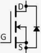
    One thing to note is that the NFET body diode is drawn incorrectly.  The polarity of the body diode should be the opposite- the anode of the diode should be at the source, and the cathode at the drain.  This means that current would flow through the body diode when the source voltage is higher than the drain voltage.  This does indeed appear to be the case in your measurements - in the "OFF" case, the source is at 3.27 V, and the drain is at 3.14 V.  

    What is the "SWITCH" node connected to?  If this has some resistance to ground, then current can flow from the OUT pin of the 555 timer, through the body diode of the FET, into the "SWITCH" node.  Otherwise, I don't know why the drain voltage would be lower than the source voltage.  It could be that the meter itself creates a path to ground, so when you measure, current is pulled through the FET.  What is the impedance of your meter you are using?

    Also, in the "OFF" case, is SW1 definitely "OPEN"?  If SW1 is not open, then current will of course flow through R7 and R8 to ground from the OUT pin.  

    Regards,
    Mike

  • Hi
    Thanks for the reply.


    • Do you have any other suggestions regarding latch circuit? I am open to any suitable idea for it.
    • Regarding diode, It is in correct polarity as you mentioned above. Cathode is towards Drain and Anode towards Source.
    • Switch Node is connected to nowhere in above testing. It will attach with GND using a switch which is CASE 3. I didn't included that case so far in the equation
    • I am using UNI-T UT55 DVM
    • SW1 is a vibration switch. It act like a push button. 
  • Ali,

    You may want to use digital devices for the latch (i.e. JK latch) and drive the LED separately.  The way you have it now, the nodes of the 555 timer are tied into both the logic functionality and the driving functionality of the FET.  Looking back on your previous description of what is required, I see that the primary function is to have a push-button function that turns an LED on-off, as well as some sort of detection of the vibration.  It appears your design is attempting to do all of these things with one 555 timer, which is admirable, but, creates a complicated solution.  I would suggest separating out the button-press function with digital devices and driving the LED separately.

    For the FET, I would have expected the drawing to look as below:

    I do think the DVM is likely the reason the drain voltage is lower than the measured source voltage.  The DVM input resistance is 10 MOhm, so it would pull some current (~300 nA) across the body diode of the FET, causing a voltage drop.  So, I don't see any reason why the current in the 555 timer would be high.  What is the current that you measure?

    Regards,
    Mike

  • Hi
    I am sorry for the confusion of diode in the picture that i sent you. I just checked that picture. In this picture it look like in reverse direction while in actual it is in correct position. Also, it doesn't matter because i create these symbols. Footprint are map in a good way so no worries about the diode direction. I also attached a pdf of schematic for better view.


    sch.pdf

  • Hi Ali,

    Ok, no problem, I just assumed it was a symbol mix-up.  What about the current?  How much current are you measuring when it is in the "OFF" state?

    Regards,
    Mike

  • Hi
    I tested with Power supply and It consumed 12mA when ON and no current show up at supply when it is OFF which might be due to resistance etc.

    With my DVM, it is not even turn ON. I ordered Fluke 170 DVM to find the current if it show up.

    As power supply showing 12mA current which is very low. A 100mA battery should last long at 8 hours.

    I will perform another test analysis with full charge battery to see if battery has some issues.

    Thanks

  • Hi Ali,

    Ok, I'll leave this thread open for now, let me know if any other questions come up.

    Regards,
    Mike