This thread has been locked.

If you have a related question, please click the "Ask a related question" button in the top right corner. The newly created question will be automatically linked to this question.

LMX2581: How to get the right frequency from the LMX2581?

Part Number: LMX2581
Hi,
I was given a certain project to lead. It was carried out by a person who is no longer with us and I have a problem finishing it.
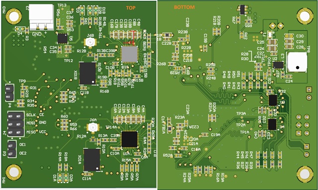
On the developed board there are 2 pieces of LMX2581. I managed to run the power supply (stable 3.28V) and establish communication with the circuits. HOWEVER, the output frequencies are incorrect. Is equal than 3.8 GHz (VCO mode) or less than set(channel divider mode).  I checked the input frequency, it is correct and equal to 100 Mhz, for both my circuits. 
 
I am sending an excerpt from the schematic I am using:


n addition, I replaced the loop original filter values with those suggested by Clock Design Tool:

I include screenshots of the settings and the resulting values:


It also shows an example of the configuration I use:

Fullscreen
1
2
3
4
5
6
7
8
9
10
11
12
13
R15 0x021FEA0F
R13 0x4080410D
R10 0x210050CA
R9 0x03C7C039
R8 0x207DDBF8
R7 0x00082317
R6 0x000004C6
R5 0x00308005
R4 0x00000004
R3 0x2000F3C3
R2 0x0C000012
R1 0xC0000081
R0 0x60A00000
XXXXXXXXXXXXXXXXXXXXXXXXXXXXXXXXXXXXXXXXXXXXXXXXXX

What would be the best way to solve the problem? is it caused by errors in Loopfilter? I apologize if I'm asking too simple questions, but this is not a topic I specialize in, so I have gaps in knowledge.

Thanx,
  • Hi Mat,

    I don't have problem locking the PLL to 2GHz using your register configuration. 

    However, your loop filter is not ideal. C3 cannot be pF. The reason is specified in the datasheet section 8.3.7. EVM original loop filter works pretty well with your configuration, you may consider to re-use it. You may increase the charge pump current if you want a little bit higher loop bandwidth.

    What kind of XO you are using? The XO is driving a small load (47R + 18R) directly, make sure you get a signal big enough for LMX2581.

  • Thank you for your reply.
    As for the filter, I have two independent circuits and two filter configurations. The first variant (similar to EVM) and the second, after my changes, it does not work properly in both.

    I checked the input clock as recommended, directly on the capacitor side of the LMX circuit. The signal I saw can be seen in the picture(ch2-color green). The amplitude of this signal is almost 1.5V.
    My XO it's ASVMB-100.000MHZ-XY-T(MEMS OSC XO 100.0000MHZ LVCMOS)

    Oscillogram(ch1- yellow) is the signal waveform(sine) of 3.8GHz, after uploading the configuration I posted above.

  • Hi Mat,

    Does your programming sequence start from R15 and end with R0?

  • Hi Noel,
    Yes, I am using the original files generated in TICS Pro(example above). We created an application to upload them to ICs. I attach an example of how it works in the picture.

    Do you think it is a problem with the programming sequence?

  • Hi Mat,

    If your programming sequence is R15, R13, R10, ...., R2, R1, R0, it should work, I did the same programming on the EVM and it worked. 

  • Unfortunately, but with me it does not work. What else can I do to determine what the problem is?

  • Hi Mat,

    Can you read back to see if you have all the registers written correctly?

    in addition, try set LD_SELECT = 7, you should see a 6.25MHz clock from LD pin.

  • Thank you for your reply. For the configuration given earlier, I changed LD_SELECT to R/2 mode, and I have a stable 6.25 MHz output.
    It seems to me that the configuration uploads correctly, the circuits respond to changes in the configuration file. Unless the problem is with the chip reset.
    Do you have any more suggestions?

    edit: Additionally, I performed measurements of all input and output voltages from the circuit. Photo attached.


    I tried to change the values of the PLL filter, an example of the appearance of the signal an input VTUNE

  • Hi Mat,

    Most of the pin voltages are correct. Vtune/CPout = 0.02V because the PLL is unlock. You can see 6.25MHz clock means you don't have issue with programming. I don't know what went wrong.

    Could you share the pcb layout?

  • Hi, thanks again for your reply.
    I am sharing a part of our PCB. We noticed some errors on the board earlier, such as routing GND to capacitors and a misplaced C23(equivalent to your C4). I marked how it was fixed, similarly in both circuits. 


  • Hi Mat, 

    Is it a two-layer pcb? I hope it is not as the loop filter is underneath the RF output traces, this may lead to RF signal loop back and interfering the VCO. You may try, during initial programming, make R3 = 0x2000F3F3, this will powerdown all the output buffers. If the VCO is locked, Vtune voltage will be around 1.2V.

  • Hi Noel.
    No, the PCB is 4 layers.
    With this setting(R3) you suggested and without it I have VTUNE 3.26 (almost VCC) at the input, but with other register settings it is 0.02V. The current draw in front of the ICs decreased, but I guess this is normal behavior with the output buffers off.
    I have replaced one of the circuits with another. The situation is still the same.