This thread has been locked.

If you have a related question, please click the "Ask a related question" button in the top right corner. The newly created question will be automatically linked to this question.

LMK04828: LMK04828 Noise floor issue on vibration

Part Number: LMK04828

Hi e2e.ti.com/.../4798065

We are also observing the same behaviour  https://e2e.ti.com/support/clock-timing-group/clock-and-timing/f/clock-timing-forum/587468/lmk04828-phase-noise-vibration on DAC39J82EVM and our custom board.

We have seen this on Y1 and CLKOUT(DCLK6) of this board.

We are observing the same on our custom board on VCXO, LMK CLK OUTPUT and DAC Output.

VCXO Used: V7223T-100.0M &  CVPD-922. In both of the VCXO we have observed. Does VC pin has a role in this issue?

We have tried changing the reducing the PLL1 PFD & Charge pump current gain and tried operating in PLL2 Mode, still we observe noise floor issue while in any vibration on board or near or due to FAN.

We would appreciate your suggestion.

  • Hi Team,

    Awaiting for your responses

  • Hi Lakshminarayana,

    I believe, you are operating the device in dual PLL mode and feeding the external reference input at CLKin0/1 input.

    The noise floor variation issue can be due the bad reference and not having appropriate PLL1 loop filter BW. I would suggest to provide the low noise reference input to PLL1 or optimized the PLL1 loop filter (reduced BW) to neglect the effect of external reference signal at PLL2 output.

    Apart from that, may be need to verify the VCXO performance at vibration on board or due to the FAN.

    Thanks!

    Regards,

    Ajeet Pal 

  • Hi Team,

    Thanks for your response.

    We are observing this issue in DAC Evaluation board DAC39J82EVM with Single PLL2 Mode with onboard CMOS VCXO CVPD-922X-122.88MHz Part.

    Attaching a clip for your reference.

    We have tried with Dual PLL mode, with a clean clock from Signal generator, we still observe the vibration noise at the LMK Output.

    We are observing the same issue on our custom board with Single PLL and Dual PLL Mode.

    Thanks.

  • Are you able to bypass the VCXO?  That is to say provide a clean 122.88 MHz input directly into the OSCin?  I know that CVHD-950-122.88 wasn't great for vibration and I'm thinking the CVPD is probably similar.

    Note when operating in single PLL2 mode, if the Vtune is floating then that could cause issues for noise too.  Best to force the Vtune.

    We have tried with Dual PLL mode, with a clean clock from Signal generator, we still observe the vibration noise at the LMK Output.

    This won't impact vibration effects from VCXO.

    73,
    Timothy

  • Hi 

    Do you suggest any alternate part to crystek which is good for vibration and with a good phase noise?

  • Hi Timoothy,

    Awaiting for your feedback,

  • Hi Lakshminarayana,

    I haven't done vibration testing on different VCXOs, however I think the smaller the package the better.  Also lower frequencies are better because the quartz is thicker.

    I think the Epson VG-4513CA/CB is good.  The datasheet for this device suggests it has excellent vibration resistance and they spec it... 1.6 ppb/G @ 20 Hz to 200 Hz.  This part is pretty good for phase noise performance to as I recall.  https://www5.epsondevice.com/en/information/technical_info/pdf/pb_vg4513.pdf

    However Epson may have some better parts since then for performance.  Now that I look at digikey, it appears this VG-4513 may be discontinued... VG7050CDN may have replaced this... there are also LVDS and LVPECL options which are nice and work with our differential input.

    Note best phase noise is often associated with smallest pull-in range.

    73,
    Timothy

  • Hi Team,

    Thanks for your response.

    Which one would you advise for LMK Input to perform better? LVCMOS, LVPECL, or LVDS Inputs? Following the optimal phase noise component that was selected.

  • I would probably pick LVPECL for all around noise floor and differential input (better for crosstalk).  LVPECL has larger swing, typically Vid = 800 mV vs LVDS, typically Vid = 350 mV to 400 mV.

    CMOS can also provide good performance due to large swing... however you do also need to use a voltage divider to take 3.3 V to sub 2.4 Vpp.  Note relatively speaking, if you consider LVPECL with Vid=800 mV, then it's relative swing is 1.6 Vpp which is less than what you can do with CMOS.

    Further, the floor of the VCXO output is not necessarily a huge impact due final performance but may have some.  If you have a phase noise plot of the VCXO, you can use the PLLatinumSim tool to load this as reference noise trace into PLL2 of LMK04828 and compare the difference in performance.

    73,
    Timothy

  • Hi Team,

    Thanks for your response.

    One more question regards to LVPECL CLK Input,

    Why TI recommends placing of two AC Caps instead of a single AC Caps at the LVPECL input,

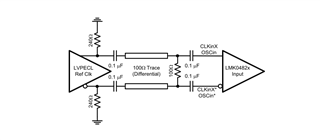
  • The output caps near the driver are to provide AC coupled output from LVPECL.  If these are not present then the emitter resistors (240 ohm in this case) are in parallel with the 100 ohm load.  This reduces their resistance.  If you do the math, it works at that 240 ohms emres in parallel with 100 ohms results in effective 120 ohm emitter resistors.  This is not necessarily bad, but you will consume higher current.

    The reason for the caps at the receiver is to allow for a offset bias on the inputs to prevent chatter when no clock is present.  For example if you removed those caps, the 100 ohms would collapse the bias and then functionality like LOS wouldn't work because there would be chatter on the input.  If this is ok with you, than you could remove the caps at the receiver.

    Of course if you remove both, then you may have common mode voltage issues depending on your receiver.

    73,
    Timothy

  • Hi Team,

    I appreciate your quick response.


    As a result, an offset will always be present with an AC coupling capacitor at the LMK input. Is it correct? What is the offset? 1.2V?


    You suggested the VCXOs VG-4513CA or VG7050CDN in a prior response to a VCXO query. However, the vibration resistance was only indicated for 20–200Hz. Would they function better with 2KHz vibration? Is LMK from TI used to test this component?


    These data might be useful to us if tested.

    Q2:

    One question on the Sinewave at LMK Input Clock standards ( i.e LVPECL Single ended Output).
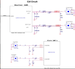
    The master LMK will supply the clock input to all of the slave LMKs in our system of multiple LMKs (Master and Slave LMK). Through a SMA Connector, the Master sends LVPECL Output while the Slave only receives Single Ended Clock IN.
    Hence Only the P output of the LVPECL will be linked to the SMA Connector at the Master, and this single ended P Output sinewave will be connected to the Slave. The negative output of the LVPECL will be terminated with a 50 Ohm termination at the Master as shown in below figure,

    Thanks.

  • Hi Team,

    Awaiting for you response.

    Thanks.

  • Hi,

    As a result, an offset will always be present with an AC coupling capacitor at the LMK input. Is it correct? What is the offset? 1.2V?

    You are thing of the DC bias, I'm referring that the DC bias at each input is slightly different so they don't chatter.

    You suggested the VCXOs VG-4513CA or VG7050CDN in a prior response to a VCXO query. However, the vibration resistance was only indicated for 20–200Hz. Would they function better with 2KHz vibration? Is LMK from TI used to test this component?

    We have not tested vibration of VCXOs.  I imagine if better in 20 to 200 Hz, then probably also better at 2 kHz.  VCXO vendors would be the people who primary test this.

    --

    Please post separate questions to separate threads.

    73,
    Timothy