This thread has been locked.

If you have a related question, please click the "Ask a related question" button in the top right corner. The newly created question will be automatically linked to this question.

LMK04821: PLL1 occasionally loses lock

Part Number: LMK04821

Hi team,

One of our customer's issues, I'm forwarding it below, could you please provide some troubleshooting suggestions

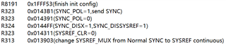
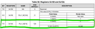
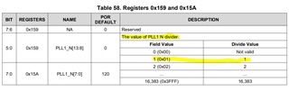
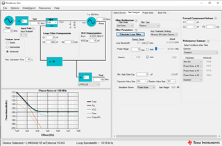
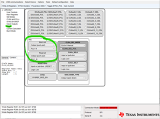
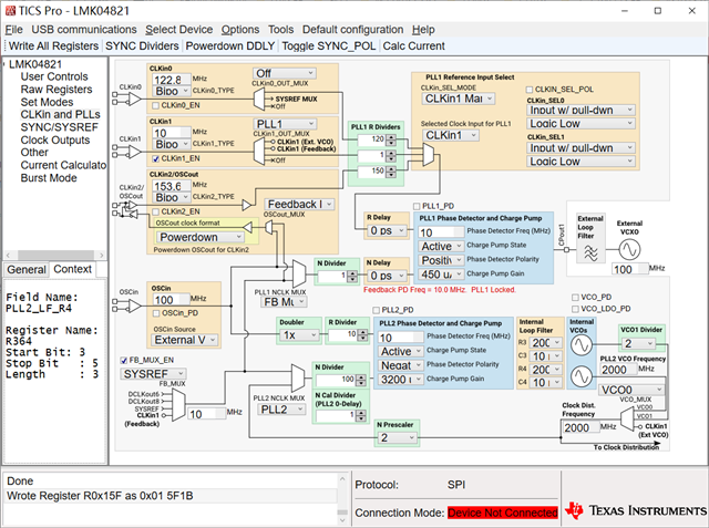
Using lmk04821, works in Dual-pll cascaded zero-delay mode, the TICS pro configuration file is lmk04821_config.tcs.The reference clock input is a 10MHz, 5dBm sine wave, input from CLKin1.Grab the PLL_DLD signal from the chip IO output via the FPGA. PLL1 was found to be occasionally out of lock, after which it was about 0.16ms then locked again; PLL2 was always locked. May I know what is the probable cause of the PLL1 being out of lock and if it is not configured in the correct way.

Best Regards,

Amy Luo

  • Hello Amy,

    After looking at your TICS Pro file, I believe the problem may be that your SYSREF is not set up correctly. If you go to the SYNC/SYSREF tab, and then look to the right of the window, your SYSREF_CLR is enabled, and it should not be if you want to have a SYSREF output (notice the message that says that in red). Make sure to uncheck that box. What is going on internally is that register ensures no unwanted pulses occur (more information about this on page 41 of the data sheet), which may be the reason your PLL1 is coming from unlocked to locked state.

    If this is not the case, I believe this lock state changes could be coming from how the external loop filter was designed. So with your reply, please make sure to include that information (resistor and capacitor values, topology used, loop bandwidth desired, and external VCO gain or data sheet) to best support you. You can also you TI's PLLatinum Sim tool to design your loop filter based on your loop bandwidth and external VCO gain (can download it here).

    Good Luck,

    Andrea

  • Hi Andrea,

    Thank you for your reply. This text is the register configuration sequence.

    lmk_cfg_value.txt
    R0 (INIT)	0x000090
    R0	0x000000
    R2	0x000200
    R3	0x000306
    R4	0x0004D0
    R5	0x00055B
    R6	0x000600
    R12	0x000C51
    R13	0x000D04
    R256	0x010001
    R257	0x010155
    R258	0x010255
    R259	0x010302
    R260	0x010422
    R261	0x010500
    R262	0x0106F1
    R263	0x010756
    R264	0x010801
    R265	0x010955
    R266	0x010A55
    R267	0x010B02
    R268	0x010C22
    R269	0x010D00
    R270	0x010EF9
    R271	0x010F66
    R272	0x011004
    R273	0x011155
    R274	0x011255
    R275	0x011300
    R276	0x011422
    R277	0x011500
    R278	0x0116F1
    R279	0x011761
    R280	0x011808
    R281	0x011955
    R282	0x011A55
    R283	0x011B00
    R284	0x011C22
    R285	0x011D00
    R286	0x011EF1
    R287	0x011F61
    R288	0x012001
    R289	0x012155
    R290	0x012255
    R291	0x012302
    R292	0x012422
    R293	0x012500
    R294	0x0126F1
    R295	0x012766
    R296	0x012801
    R297	0x012955
    R298	0x012A55
    R299	0x012B02
    R300	0x012C22
    R301	0x012D00
    R302	0x012EF1
    R303	0x012F66
    R304	0x013001
    R305	0x013155
    R306	0x013255
    R307	0x013302
    R308	0x013422
    R309	0x013500
    R310	0x0136F1
    R311	0x013736
    R312	0x013810
    R313	0x013900
    R314	0x013A00
    R315	0x013BC8
    R316	0x013C00
    R317	0x013D00
    R318	0x013E03
    R319	0x013F0D
    R320	0x014009
    R321	0x014100
    R322	0x014200
    R323	0x014391
    R324	0x014400
    R325	0x01457F
    R326	0x014610
    R327	0x01471B
    R328	0x014802
    R329	0x014942
    R330	0x014A02
    R331	0x014B16
    R332	0x014C00
    R333	0x014D00
    R334	0x014EC0
    R335	0x014F7F
    R336	0x015003
    R337	0x015102
    R338	0x015200
    R339	0x015300
    R340	0x015478
    R341	0x015500
    R342	0x015601
    R343	0x015700
    R344	0x015896
    R345	0x015900
    R346	0x015A01
    R347	0x015BD4
    R348	0x015C20
    R349	0x015D00
    R350	0x015E00
    R351	0x015F1B
    R352	0x016000
    R353	0x01610A
    R354	0x016224
    R355	0x016300
    R356	0x016400
    R357	0x016501
    R369	0x0171AA
    R370	0x017202
    R371	0x017300
    R372	0x017400
    R380	0x017C15
    R381	0x017D33
    R358	0x016600
    R359	0x016700
    R360	0x016864
    R361	0x016959
    R362	0x016A20
    R363	0x016B00
    R364	0x016C00
    R365	0x016D00
    R366	0x016E13
    R8189	0x1FFD00
    R8190	0x1FFE00
    R8191	0x1FFF53(finish init config)
    R323	0x0143B1(SYNC_POL=1,send SYNC)
    R323	0x014391(SYNC_POL=0)
    R324	0x0144FF(SYNC_DISX=1,SYNC_DISSYSREF=1)
    R323	0x014311(SYSREF_CLR=0)
    R313	0x013903(change SYSREF_MUX from Normal SYNC to SYSREF continuous)
    

    And the final TICS pro configuration file is lmk_cfg_final.tcs

    I have set SYSREF_CLR to 0 in the final configuration as shown below.

    The schematic about the external circuit of the lmk04821 is SCHEMATIC-LMK04821.pdf. And the datasheet for the PLL1 external VCXO is CVHD-950 datasheet.pdf. Please help to confirm if there is a problem with the hardware design.

    In addition, the datasheet has requirements on the slope of the input reference clock, whether it will cause the PLL1 to lose lock sometimes. Now the reference clock input is a 10MHz, 5dBm sine wave, input from CLKin1.

    Best Regards,

    Xiaoyang Guo

  • Connecting OSCinP to GND with a 0.1uF capacitor doesn't solve this problem. PLL1 loss of lock seems to be related to external interference. For example, If I adjust the knob of the fan that cools the board, PLL1 will lose its lock.

    I use the oscilloscope to trigger PLL1 to lose lock and observe the Vtune pin of VCXO as shown in the figure below. Wherein, yellow is PLL lock loss signal and blue is Vtune signal.

  • Hello Guo,

    After looking over your TICS Pro, the data sheet, and running my own loop filter design simulations, there seems to be three problems:

    1) Even though I know TICS Pro says otherwise and doesn't show an error, the N-Divider does not accept N = 1 values. This can lead PLL1 to unlock. This information can be found in the data sheet on p. 85 and on my screenshot below. Therefore, I have also included my TICS Pro file, to give a suggestion to your own file  LMK04821_PLL1Lock_LoopFilter.tcs..

    2) When I inputted your loop filter into PLLatinum Sim with Fpd, CLKin1 frequencies, and charge pump current as shown in your TICS Pro file, I got a very low phase margin, making your design unstable and causing your PLL1 to unlock. If all that is correct and you are aiming to obtain a loop bandwidth of 0.166 kHz, then I would recommend you use C1539 = 3.9 nF, C1538 = 180 nF, and R138 = 18 kΩ if you decide to keep Fpd = 5MHz (as I demonstrated in my attached TICS Pro file). If you would like further help on this design, please let me know what loop bandwidth you are aiming to achieve.

    3) Regarding the slew rate consideration you mentioned, from my calculations, you are not hitting the minimum requirements for slew rate on the data sheet, which is expected when using sine waves. This could also be a reason your PLL is not locking.

    Good Luck,

    Andrea

  • Hi Andrea,

    I think PLL1_N can be set to 1 according to datasheet, and the right side of the table below shows the value range of PLL1_N[13:0].

    I found that the phase margin of PLL1‘s loop filter before is really small, only about 10 degrees. And I use PLLatinum Sim to adjust loop filter to obtain the phase margin of 70 degree like the screenshot below. However, when I test it on board, the frequency of PLL1 losing lock is higher. I don't understand it and guess maybe something wrong when i use PLLatinum Sim. Cause i configure lmk04821 in nested dual-pll 0-delay mode, the pll1's feedback is sysref but not oscin, and PLLatinum Sim seems can't simulate dual-pll mode, I would like to ask how to calculate the loop filter with  PLLatinum Sim in this case.

    Best Regards,

    Xiaoyang Guo

  • Hello Xiaoyang,

    You are correct, PLLatinum Sim can only do one PLL simulation at a time, and it cannot be configured in SYSREF and Dual-PLL mode. However, for the loop filter, only the Fpd, charge pump current and VCO gain matter, so the values of the dividers are not important. However, you do want to keep in mind that if you change the output frequency, you also have to change the VCO gain (i.e if your VCO frequency is 100 MHz and you VCO gain is 0.0025 MHz/V and you change to 10 MHZ VCO frequency, then you have to change your VCO gain to 0.00025 MHz/V).

    I have a few other ideas as to why your PLL1 is still not locking:

    1) Based on your input waveform, your slew rate seems to be lower than the minimum recommended spec (I'm calculating 0.0765 V/ns and the minimum is 0.15 V/ns). This can cause you PLL to unlock. I would suggest you change your signal to a square wave.

    2) If your input is spurious, I would suggest you increase your N and R dividers to divide down that unwarted signal. For instance you can make Fpd = 1 MHz, and your dividers to R = N =1. You would also have to change your loop filter to C1539 = 2.2 nF, C1538 = 100 nF, and R138 = 56 kΩ.

    3) If you changed the PLL1 window size to lower than 43 ns, I would suggest you raise it again and make it as big as possible (43 ns is the max). This can lead to longer range of locking, which could solve your problem. 

    If none of that works, I would suggest to physically check with a voltmeter your VCO voltage and see if its Vcc/2. If so, your PLLs are locking and its just a problem with the hardware. If that checks out, then I would suggest to change your "Other" settings under "I/Os." The PLL1 LD and PLL2 LD can be set to output the PLL1_N and PLL1_R (as shown in the picture below) and that would route those signals coming out of those nodes to a scope.

    I would also suggest going through this link that goes over general ideas of what to do if your PLLs are out of phase.

  • Hi Andrea,

    When I increased the amplitude of the reference clock input to 10dBm, the frequency of PLL1 lost lock decreased significantly. And when the reference clock input is 10MHz square wave or 250MHz sine wave, PLL1 doesn't lose lock. So it seems that the insufficient slew rate of the input clock is the main reason why PLL1 sometimes loses lock. Thank you for your suggest.

    Furthermore, in my understand, the PLL1_N and PLL1_R are values but not flags, i don't understand the PLL1 LD and PLL2 LD mean when setting them to output PLL1_N and PLL1_R. I didn't find relevant information in the datasheet. Could you please explain it.

    Best wishes,

    Xiaoyang Guo

  • Hello Xiaoyang,

    I am glad those recommendations worked. PLL1 LD and PLL2 LD, by default, refer to the two LED lights telling you if PLL1 and PLL2 are locked. That drop down menu allows you to change the default and have other values/states/signals be routed through those pins. If you set PLL1 LD to PLL1 N, the signal coming out of PLL1's N divider will be routed through that pin, Therefore, you can connect those pins to an oscilloscope and see the signal at that node. I believe the EVM even has test points for those nodes so you don't have to solder the board. Hope this helps!

    Best,

    Andrea

  • Hi Andrea,

    Thank you for your support. The customer hasn't followed up for a long time and I think the issue has been resolved