This thread has been locked.

If you have a related question, please click the "Ask a related question" button in the top right corner. The newly created question will be automatically linked to this question.

CDCLVC1104: Input Capacitance

Part Number: CDCLVC1104
Other Parts Discussed in Thread: CDCLVC1108, CDCM6208

We are working at selecting an external clock source for the CLKIN inputs.
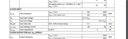
The datasheet only specifies the slew rate for the inputs (1~4V/ns)

Can I get an answer on the following parameters for the device please?
(For both CDCLVC1104 and CDCLVC1108)

1) The CLKIN signal voltage should be between GND ~ VDD and needs to meet VIH / VIL specs from section 6.3 right?

2) What voltage level is the slew rate (tr/tf) specified for? (20%~80%Vcc or 10%~90%Vcc?)

3) What is the max input capacitance of the CLKIN pin? (according to this E2E post typ is 2pF)

4) As long as the min pulse width (low and high pulse width) specified in 6.3 is met, does duty cycle matter? (45%~55% duty cycle limit, etc)

Regards,
Darren

  • Hi Darren,

    1) The CLKIN signal voltage should be between GND ~ VDD and needs to meet VIH / VIL specs from section 6.3 right?

    Correct, it should meet the VIH and VIL requirements. 

    2) What voltage level is the slew rate (tr/tf) specified for? (20%~80%Vcc or 10%~90%Vcc?)

    Rise and Fall time is defined for 20% to 80%. Slew rate is usually the slope at any point in the waveform. So its a little different than rise and fall time.

    3) What is the max input capacitance of the CLKIN pin? (according to this E2E post typ is 2pF)

    Input capacitance at schematic level is listed below, considering layout parasitic, maximum value would be higher around 2-3pF.

    Typical input capacitance CIN_SE

     1.095pF

    Maximum input capacitance CIN_SE

     1.267pF

    As long as the min pulse width (low and high pulse width) specified in 6.3 is met, does duty cycle matter? (45%~55% duty cycle limit, etc)

    The pulse width low and high with duty cycle limit should give correct output. If you have low and high pulse width with different duty cycle then low and high pulse width would be different.

    Best,

    Asim

  • Hi Asim,

    Regarding the Slew Rate.
    Normally the output impedance of the clock source, and the input capacitance of the CLKIN pin create an RC time-constant that slows the input clock edge.
    If the design has no overshoot, then there is a "rounding" of the edge as it approaches V_OH (output high) for a rising-transition.

    I believe there should be some input voltage range the slew rate is specified for.
    For example, the slew rate needs to be 1~4V/ns for the rising/falling edge at is passes the threshold voltage.

    The exact threshold voltage varies across PVT, so usually we use the input high/low max-min values to get the range requirements.
    Datasheets usually spec the Slew Rate from 20%~80%Vcc to give an idea of the critical slew rate when passing the threshold voltage.

    For example, see Table 6.14 in the CDCM6208 datasheet (link) where the output slew rate is specifed for a specific voltage range and load capacitance.

    Can you double-check and see what the required input range for the slew rate is? (20%~80%Vcc is typical)

    Regarding the minimum pulse width.
    Do I understand correctly that whatever the input duty cycle is, the output duty cycle will be the same?

    So let's say 25MHz input clock has an ideal 0[ns] rise/fall time.
    The pulse width (tpw) for an ideal 50% duty cycle = 20ns (20ns High and Low = 40ns total = 25MHz)
    But now let's add some duty cycle error (±10% = 40%~60%) because nothing is ideal.

    Now tpw_high = 22[ns] and tpw_low = 18[ns].
    Will the output duty cycle be the same as this input duty cycle, or will it be different?

    Is there a required input max. duty cycle limit?

    Regards,
    Darren

  • Hi Darren,

    Input slew rate range is specified for 20 to 80% of input swing.

    Do I understand correctly that whatever the input duty cycle is, the output duty cycle will be the same?

    Yes, that's correct. Output duty cycle variation is  45% to 55% based on 50% input duty cycle which is ±5% duty cycle distortion. In case of 22ns we would add the ±5% duty cycle distortion and that would be your output duty cycle. So 22ns ±1.1ns would be tpw_high. Same goes for tpw_low.

    Let me know if this clarifies your question.

    Best,

    Asim

  • Hi Asim,

    Just to clarify.

    1) The datasheet doesn't list the clock input slew rate as 20~80% of input swing, as your attached image shows.
    Where does this come from, and am I safe in understanding this also applies to all cdclvc11xx family devices?

    2) I understand the clock buffer is different from a clock generator which reconstructs an output clock using internal PLL, etc.
    Because of this, the output duty cycle tracks the input duty cycle, with added degradation due to the pulse width (tpLH - tpHL) skew.

    I have attached an excel sheet with some super simple calculations to understand duty cycle degradation.
    Is my understanding correct?

    For example, considering the following:

    VDD = 2.5V
    f_in = 125MHz
    p_skew = 220ns (because VDD = 2.5V)

    Here, assuming 50% input duty cycle, the expected max degradation is ±2.75%, right?

    The ±5% you gave in your example above, is because at the "max" conditions:

    VDD = 3.3V
    f_in = 250MHz
    p_skew = 180ns (because VDD = 3.3V)

    We get a max duty cycle degradation of ±4.5%, right?
    (Can also be confirmed using the attached excel sheet)

    duty_cycle_degradation.xlsx

    Regards,
    Darren

  • Hi Darren,

    1. Sorry for the wrong datasheet reference. I mentioned LMK1Cxxx family there which is latest revision of CDCLVC1XXX family. But for CDCLVC1XXX, its 20% to 80% as well.

     2. I checked the datasheet requirements again. Yes, its defined based on maximum or worst case conditions. But if you explicitly consider the the 2.5V then it changes to  ± 2.75% as you mentioned in your comments. Excel sheet is correct based on both assumptions.

    Best,

    Asim