This thread has been locked.

If you have a related question, please click the "Ask a related question" button in the top right corner. The newly created question will be automatically linked to this question.

CDCE62002: int EEPROM to RAM load issue

Part Number: CDCE62002

Hi i have few quesitons related the datasheet instruction about EEPROM to RAM loading,

Cite from Datasheet -

Note: The SPI_LE signal has to be high in order for
the EEPROM to load correctly into RAM on the Rising edge of PD^. - Question #1: we havn't found any instruction of what is the time the SPI_LE should be on before the rising of PD^

About the Timing Requirements:

Maximum shunt capacitance: Max 7 pF - Question #2: what is this capacitor where is it placed?

PD REQUIREMENTS
tr / tf Rise and fall time of the PD signal from 20% to 80% of VCC Max 4 ns - Question #3 does it mean that the PD shall rise at the rate of no more than 4 ns?

Thanks 

Arye

  • Arye,

    1. In the "Pin Functions" section of the datasheet, there is some guidance offered on the timing: "The SPI_LE signal has to be high in order for the EEPROM to load correctly on the Rising edge of PD". I would interpret this as meaning that the SPI_LE signal must be at least 0.7 * VCC by the time that the PD signal is at 0.2 * VCC. The built-in pull-up resistor on the SPI_LE pin is enough for this task., assuming that PD is not issued before VCC

    2. This is with regard to the auxiliary input pin, AUX_IN. This is not used in most cases.

    3. The time that it takes for the PD signal to rise or fall from 20% to 80% of VCC must not exceed 4 ns.

    Thanks,

    Kadeem

  • Hi Kadeem,

    thank you very much for your fast reposne, both lines PD_ and SPI_LE have 150kohm pullup so if both start to rise on power up, they should go up together.

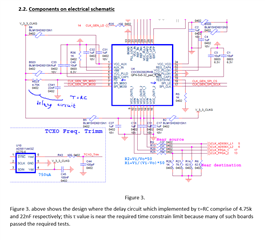
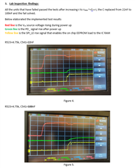
    please see my schema and our lab results, we had few products with failure probobly in the EEPROM load to RAM

    replacing our cap from 22n to 100n solved the failure of these cards proper power up, yet i think we are not comply with the 4 ns in our design, would be glad if you could recommand for us for the right steps that will make sure our design will not have any failures

  • Arye,

    Glad to hear that increasing the PDN capacitance resolves the issue - we have seen in some cases that increasing this capacitance may be required for successful part startup.

    It is difficult to tell in the pgoto if the timing spec is being violated; however, if the power up is now completely successful, it is likely no longer an issue.

    Thanks,

    Kadeem

  • Hi thanks Kadeem,

    the picture shows that the time per square is 1ms, which means the rise time of PD_ is much more than 4ns.

    i hope guess from your response above that it means that if the power up finished successfuly it does mean this kind of solution is fine.

    Tnx,

    Arye

  • Arte,

    So long as the output clocks are consistently coming up properly on startup, this should not be an issue.

    Thanks,

    Kadeem