This thread has been locked.

If you have a related question, please click the "Ask a related question" button in the top right corner. The newly created question will be automatically linked to this question.

LMX2572: Getting phase-coherent behavior of multiple frequencies

Part Number: LMX2572
Other Parts Discussed in Thread: LMX2581

Hello, this is a follow-up question to this:
https://e2e.ti.com/support/clock-timing-group/clock-and-timing/f/clock-timing-forum/1278540/trf3765-getting-phase-coherent-behavior-of-multiple-frequencies-out-of-trf3765/4857650

We're using multiple LMX2572 PLLs, that we want to have phase-coherent to each other, but also to a reference frequency (e.g. the input frequency of PLL), that all are phase-aligned to the zero-phase point of the PLL.

The desired operating frequency is the ISM Band between 2.4 GHz and 2.5 GHz. Unforunatly, this wasn't doable without a channel divider. As stated in the datasheet (page 17/90):
"To go below the VCO lower bound of 3.2 GHz, the channel divider can be used". Ideally, we would like to bypass this, since we only want to use an integer PLL (e.g. 100MHz * (N = 24) = 2,4GHz)

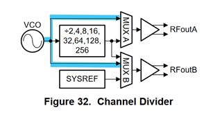
Question 1: Is there a way to get this without the Channel Divider, that we're missing in the datasheet?

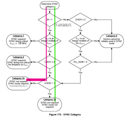
As suggested by the datasheet (page 67/90):

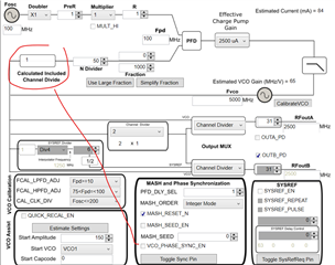
Red path: We set CHDIV = 0 (Which gives a channel divider value of 2 for the equation)

We set:
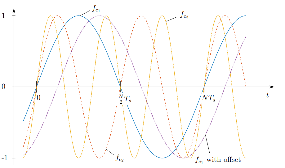
1. (PLL_N = 50, PLL_NUM = 0 & PLL_DEN = 1000) to result (2,5GHz) --> Channel 1 (Yellow)
2. (PLL_N = 48, PLL_NUM = 0 & PLL_DEN = 1000) to result (2,4GHz) --> Channel 2 (Blue)
For the equation: resFreq = refFreq *(PLL_N + PLL_NUM / PLL_DEN) / Channel Divider

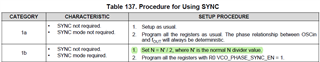
This worked fine, but the SYNC Mode didn't work as expected. We set register R0 (offset: 00h) as suggested after reset to (2118h) then to (6118h). By this setting (VCO_PHASE_SYNC_EN = 1)
Question 2: How to exactly activate SYNC Mode, other than just setting this bit? We are getting a bizzar behavior like jumping frequency and amplitude, so not a reliable frequency as without this bit set.

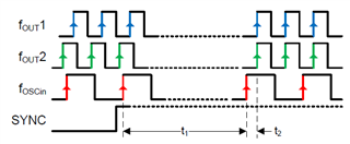
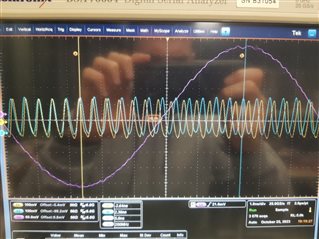
Instead we got, by the nature of the integer PLL, a synchronous behavior to the reference frequency, that was only reproducible after re-powering with an offset. Please see the pictures below:

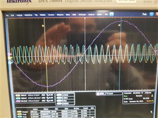
We think, this might be due to the nature of the channel divider.
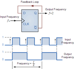
By feeding back the Q' into the D Flip-Flop, the frequency gets clock divided by two, but the it depends on the intialial value of D, whether the output Q is negated in reference tothe clock or not.

Question 3: Would you maybe give an insight, how your channel divider operates? If these are as we think, then the output can only have two form and 180° offset. Could we manipulate the input of the input, to get always a similar result after repowering?
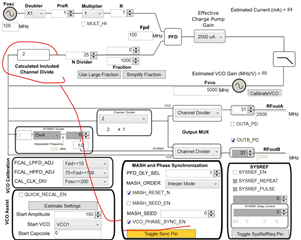
Green path:

Question 4:Why is setting CHDIV to 1 (so Channel Divider = 4) wouldn't need any Sync feature?

  • Hi Danny,

    The VCOs in LMX2572 cover 3.2GHz to 6.4GHz, a channel divider is necessary in order to get 2.5GHz.

    As you pointed out in the flow chart, you are in CAT.1b sync. You don't need a sync signal but you need to enable sync mode.

    Please note there is a Included Channel Divide in the feedback path. Before making VCO_PHASE_SYNC_EN = 1, this divider value is =1. N divider = 50 for 2500MHz. 

    Once this sync enable bit is set, this divider value =2. Now, the N-divider = 25.

    Datasheet has this instruction.

    You are right, with div/2 output, there will be two distinct phases: 0 or 180deg. By making the sync bit =1 with div/2, we are taking the div/2 signal (from the Included Channel Divide) back to the PLL, so the div/2 problem from Channel Divider gets cancelled out. With other CHDIV values, we need to use the internal re-clocking circuit to maintain a constant phase, as a result, we need a sync signal to trigger the re-clocking circuit. 

    If your application is stick to integer channel (PLL NUM = 0), you can use LMX2581 to get direct VCO output, then you don't need sync anymore. 

  • Hallo Noel, thanks for the quick reply and the pictures!

    I'm not using the provided software, but I'm able to write the registers via SPI with my own GUI. I indeed knew about the "Calculated Included Channel Divide" and I got the SYNC-Mode working for now. All this do is just choose one of the two options (0 or 180deg, not sure which one exactly) and the formula for the output frequency is as follows:

    outFreq = refFreq * (SYNC_Mode_Bit +1) *(PLL_N + PLL_NUM / PLL_DEN) / CHDIV
    All this is clear. I'm just not sure, if my the phase sync is accurate enough for my application.
    I let it run on 2.5GHz in SYNC Mode (so N=25 as your setup) and
    it was synchronous to the 100MHz (triggered at zero-crossing point rising edge) and
    the PLL output frequency was hitting the exact same zero-crossing point but in falling edge.
    I then noticed the signal drifting almost 50ps to the left and later 100ps. Is this normal?
    My signal generator is operating at +4dBm and produces a fairly stable frequency.

    For my application, it is important, that re-powering and writing the exact same registers with the same values, should produce no change in phase from one PLL frequency to reference frequency (e.g. always 130°, so a static phase delay only).

    I also wanted to ask you about some registers:

    1. R37 (Offset: 25h)
    With f_VCO = 100MHz * (N = 23) = 2.3GHz: Should I choose according to Table 3 PFD_DLY_SEL 0 or 1?
    I am orienting myself by f_VCO, so this should be 0, but according to N it should be 1.

    2. R58 (Offset: 3Ah)
    INPIN_FMT is a somehow weird, since 0 & 4 are identical. Does it matter, what the SYNC type is for SYNC-Mode? Since it's mentioned before, that an async. SYNC pulse is sent, when toggeling the VCO_PHASE_SYNC_EN from 0 to 1.

    Back to the green path from the diagram:

    I tried my best to get the VCO to lock at any frequency with CHDIV=1 (so Channel Divider value is 4), but it only locked with 1.5GHz (That is N=60 and in SYNC-Mode N=30). Other than that, the frequency never got stable. Do you maybe have an idea, why this happened? I'm still confused, why you would need no SYNC nor SYNC-Mode at this case?

    Thank you for the suggestion of LMX2581. This seems to have a signle-ended input reference input clock. I need something like the LMX2572 with a differential input clock. We have a lot of channels, so the price has to be suitable too.

  • Hi Danny,

    Phase synchronization means after sync, there is a deterministic phase between input and output, t2 in below diagram. This phase difference is due to the propagation delay. In your use case in Cat.1b sync, every time you power up the device and program it with the sync enable bit=1, you will get pretty much the same amount of t1. This delay is temperature dependent, it is very likely that you will see the delay is changing after the device is heating up. 

    When we determine PFD_DLY_SEL value, we should use VCO frequency, but not output frequency. If you have set MASH_ORDER = integer, then PFD_DLY_SEL should be 1. 

    INPIN_FMT is used to setup the expected input signal format at the SYNC pin (pin 5). Cat.1b sync does not need a sync signal, it does not matter how do you setup INPIN_FMT.

    When VCO_PHASE_SYNC_EN = 0, you should be able to get any frequency between 800MHz and 1.6GHz with div/4 output. 

    When VCO_PHASE_SYNC_EN = 1, because of Included Channel Divide and the min. N-divider restriction, N-divider cannot be smaller than 20 (MASH_ORDER = integer), so the min. output frequency is restricted to 1000MHz.

  • Hey Noel, thank you for the detailed explanation!

    So if I get this correct, the t1 delay (after the device is heating up) would only mean a whole period delay. t1 is only the delay of n-periods, as the diagram describes. That means, without affecting the synchronization of the reference clock to the output reference (e.g. 130° would still hold)? Because this wasn't the case here. Is there anyway to guarantee an acutal deterministic delay even after the device has operated? Otherwise, I would argue, that the sync-feature isn't that reliable here

  • Hi Danny,

    Oh, sorry, there was a typo.

    .........you will get pretty much the same amount of t1t2.

    t1 is the time taken to complete synchronization in Cat.2 and 3 sync. 

    Cat.1a and 1b do not have t1. After programming the device, there will be a deterministic delay between output and input. We didn't do a very precise measurement on the delay over temperature, it is roughly equal to +2.5 ps/°C. Unfortunately there is no way to confine this delay, this is pretty much depending on the chip design, but we can use the phase adjustment function to manually readjust the phase. See datasheet section 7.3.12 for details.

  • Hey Noel,

    thank you for the clarification! You suggested phase adjustment, but I already gave up on that after setting "Integer Mode". This is according to the datasheet not tan option in this case (which is also understandable due to the nature of the Integer-PLL). Page (19/90):

    There are a couple of restrictions when using phase adjustment:
    • Phase adjustment does not work with MASH_ORDER equals 0 (Integer mode) or 1 (First order).
    • Phase adjustment is possible with integer channels (PLL_NUM = 0) as long as MASH_ORDER is greater
    than 1.
    • PLL_DEN must be greater than PLL_NUM + MASH_SEED

    So I can try to set this to a higher MASH-ORDER, but I don't want to get weird effects and being able to synchronize automatically, like it's the case now. My prefered setup would be like this with the slowest frequency being my 100MHz reference clock and all other frequencies going through the zero-point simultaneously without a phase delay (hence the phase coherent cirteria I mentioned):

  • Hi Danny,

    Right, phase adjustment has restrictions.