This thread has been locked.
If you have a related question, please click the "Ask a related question" button in the top right corner. The newly created question will be automatically linked to this question.
Team,
My customer has the following question.
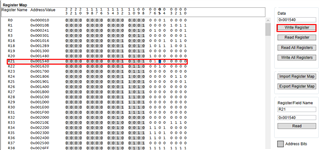
We have a question on the EEPROM of the LMK5C33216. It is working properly and we can read/write to it.
What we want to do is sanitize it, which means doing some known read and writes to verify the state of all NVM/EEPROM registers.
Our dilemma is if we write to a particular clock output and set all of it’s registers to 0x00 or 0xFF it shuts off the clock to the FPGA which is controlling/writing to the LMK.
Does the team know of a way to write to the NVM directly, without interrupting the clock(s), such that we can keep the clocks running and hence the FPGA running?
Regards,
Aaron
Hi Aaron,
You may use the SRAM Direct Write Method. This allows you to write to the SRAM directly without disturbing the current register settings. The SRAM then gets translated to the EEPROM. Refer to this PDF for more guidance.
5707.Programming LMK5Cxxxxx, LMK5Bxxxxx_Nov32023.pdf
Regards,
Jennifer
Thank you for suggesting the SRAM Direct Write Method. For a quick method of writing 0xFF to all EEPROM registers, would NVMERASE work?
For example, would the following register writes cause EEPROM memory all to go to 0xFF?
Write 0x00B4EA # NVM Prog Unlock
Write 0x00AB02 # NVM Erase Start
Hi Chase,
Let me check on it this week. Please note that setting the EEPROM to all 0xFF is not recommended if the customer plans to start-up from EEPROM (EEPROM overlay is enabled).
Regards,
Jennifer
Hi Jennifer,
Thanks for taking a look at the erase method, but for now I think I have a way of writing 0xFF to nearly all non-reserved registers. The one register that I don't seem to be able to set is bit 6 of R21.
I am currently running the following
Write R25 0x001901 # Sync Enable
Write R21 0x001540 # Software Sync Assertion
When reading back R21, I have only seen it return a value of 0x00. Does R21 immediately revert to a value of 0x00 after a sync assert, or is there something else I can do to set the 6th bit of R21 to a 1 and read it back?
Hi Chase,
When writing with SRAM method, power cycle is needed to update register values before reading back.
Did you power cycle then read back R21?
-Riley
Hi Riley,
I have tried power cycling after completing the following two writes, but even after the power cycle, 0x0015 reads back a value of 0x00.
Write R25 0x001901 # SYNC_EN=1
Write R21 0x001540 # SYNC_SW=1
However, I was under the impression that those two writes would be done by the REGCOMMIT method, as I am writing to 0x0019 and 0x0015 individually.
If I wanted to write the value 0x40 to 0x0015 via SRAM method, should the following do the trick? (I have tried this SRAM method unsuccessfully as well)
R20 0x001480
R40 0x00AB40
R173 0x00AD00
R174 0x00AE0F #SYNC_SW
R176 0x00B040 #SYNC_SW=1
R180 0x00B4EA
R171 0x00AB03
R180 0x00B400
Power cycle and read 0x0015, but it returns 0x00, not 0x40.
Am I missing something in either my REGCOMMIT or SRAM method attempts to write the value 0x40 to 0x0015?
Hi Riley,
I am able to set R21 using the TICS Pro software on a the LMK5C33216EVM dev board. However, when I try to do the equivalent register write on my target circuit board, I have not been able to write 0x40 to R21.
Would there be any other registers or HW configuration that would prevent me from writing 0x40 to R21?
Hi Chase,
Programming the device can be done through 2 methods:
- direct write on LMK registers (or REGCOMMIT method). This uses LMK register map as shown in the programing manual.
- SRAM method which uses SRAM/EEPROM register map that is different from LMK register map.
Address on SYNC_SW on:
- LMK register map: R21 (offset 0x15) bit 6
- SRAM/EEPROM register map: address 15 (0xF) bit 7
So to access SYNC_SW through SRAM write, you would need to access address 0xF with the following steps:
R20 0x001480
R40 0x00AB40
R173 0x00AD00
R174 0x00AE0F #SYNC_SW
R176 0x00B080 #SYNC_SW=1
R180 0x00B4EA
R171 0x00AB03
R180 0x00B400
Let me know if this works.
-Riley
Hi Riley,
Thanks for detailing the alternative register map for SRAM programming, but following these register writes still didn't set R21's bit 6 high.
R20 0x001480
R40 0x00AB40
R173 0x00AD00
R174 0x00AE0F #SYNC_SW
R176 0x00B080 #SYNC_SW=1
R180 0x00B4EA
R171 0x00AB03
R180 0x00B400
(then a power cycle before reading R21)
Hi Chase,
Looks like both programming ways work on the EVM but not your target board yet.
I'd need to discuss internally and get back to you.
Does this only happen with SYNC_SW or also others? For example if you could program EEREV and confirm the communication with your board that SRAM does update this EEREV properly?
-Riley
Hi Riley,
I have only been seeing this issue with SYNC_SW. All other EEPROM bits I have been able to toggle between 1's and 0's either by the SRAM method or REGCOMMIT method. Thanks for helping me debug this issue and bringing it back to your team.
As a follow-up, I am seeing similar behavior on TICS as I am on my target.
This only happens when I open USB Communications>Interface and set the Protocol to SPI_CLKLOW.
Then, when I Write Register 0x001540 then Read Register, it returns 0x001500.
Are there any other registers that need to be set while using the SPI_CLKLOW interface to enable 0x0015 to stay at a value of 0x40, or do you know why this behavior occurs?
Hi Chase,
Thanks for narrowing down to SPI. I've checked this through I2C and no issue. I will duplicate the issue with SPI and get back with my observations.
-Riley