This thread has been locked.

If you have a related question, please click the "Ask a related question" button in the top right corner. The newly created question will be automatically linked to this question.

CDCDB2000: Assembly Verification

Part Number: CDCDB2000

Hi, 

We have used 2 CDCDB2000NPPR buffers in our current design. Both the buffers were not providing any outputs. We checked all control signals from our end and everything seemed fine.

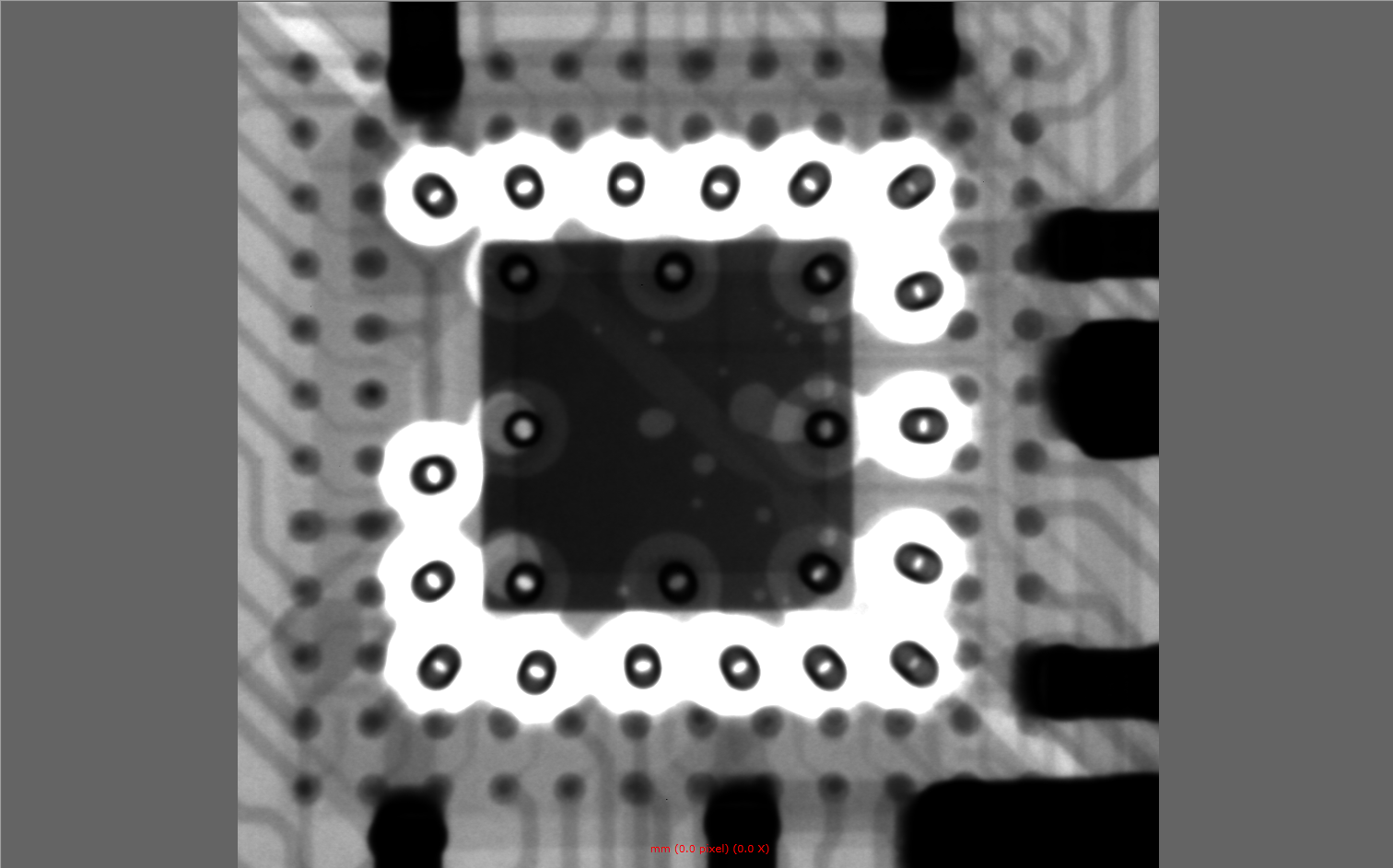
Hence, we took an X-RAY inspection of the buffers.

Attached are the X-RAY images.
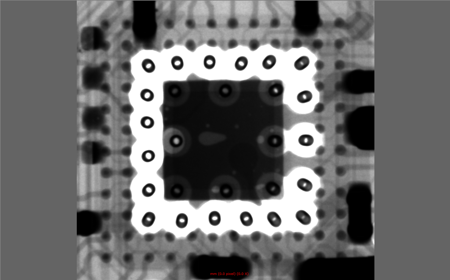
The buffers are EU25 and EU22. I am also attaching the layout of each.

Kindly see if the solderability is proper or not. Is some kind of assembly issue affecting the buffer?

Regards,

Ashbin

C-DOT

  • Hello Ashbin,

    Could you attach the schematic as well?

    Best,

    Andrea

  • Hi Andrea

    PFA Sch. page corresponding to one of the buffers - EU25.

    CDCDB2000_Sch.pdf

    Regards,

    Ashbin

  • Hello Ashbin,

    I'm checking with my team to see if they have any feedback on the X-RAY images. In the meantime, how is the customer driving the OE pins and the PWRGD/PWRDDN pins? Are they being driven high or low?

    Also, what is the swing and biasing done on the input signals to the CDCDB2000? I would like to know the signal being fed into the buffer.

    Best,

    Andrea

  • Hello Ashbin,

    I have a follow up from my team and we have a few follow up questions/actions to be done:

    1) Please take X-rays on good units and boards for EU25 & EU22 so we can have a good comparison and further debug.

    2.) Can you please complete an an ABA swap. In other words, please put these 2 units on known good boards and solder known good units on these suspected boards to see if the issue follows the unit or the board.

    Thanks!

    Best,

    Andrea

  • Hi Andrea,

    Pls see the below points:

    1. We have only 3 boards in this proto phase and the issue is there across all the 3 boards, on both buffers in each of them. So there is no way to take X-RAY and compare.
    2. I request you to forward the X-RAY images to specialists in board assembly section to get their input on the same.
    3. The OE pin is driven LOW continuously and the PWRGD pin is driven LOW-to-HIGH. Both are done by CPLD. As you know, the OE pins are there for only few of the outputs. The other outputs are also not coming. Ideally those should come. 
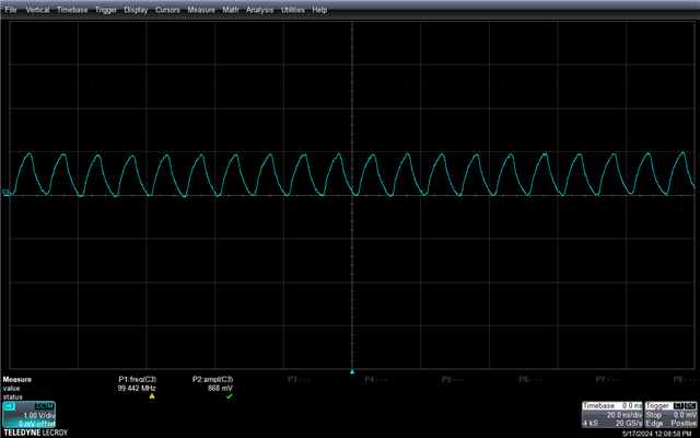
    4. The input clock swing and frequency are both fine. We have another PCIe buffer on board from Renesas - 9ZX21201BKLFT. It receives a similar clock and generates the outputs as expected. I am attaching the input clock capture from MSO.
    5. We are not able to detect these 2 buffers using I2C as well. The Renesas buffer is detected. 
    6. Kindly let us know if any specific assembly instructions. reflow profile etc are there for the buffers or not.

    Regards,

    Ashbin

  • Hello Ashbin,

    My follow-up questions came from the assembly expert in my team.  He originally mentioned that it's hard to tell what the dark shadow is in the X-RAY picture, which is why we wanted functioning devices so we could compare. I'll reach out back to him with your responses. For further debugging, can you:

    1. tell me how much current the CDCDB2000 parts are drawing
    2. check the voltage levels on the voltage pins, want to see if the voltage pins are all receiving the correct voltage.
    3. check the voltage at each OE pin, mainly the ones resulting in no outputs.

    Follow up questions:

    1. Which outputs are you not seeing an output and in which ones are you seeing an output?
    2. Which address are set for each device via the SMBus? Are they all different between all the parts?
    3. Do pins L5 and L4 have external pullup resistors?
    4. Are all 6 CDCDB2000 across the 3 boards resulting in the same exact problem?

    Best,

    Andrea

  • Hi Andrea,

    First of all let me tell you it has been a week since the issue was reported and you are replying once in a day, that too after our office hours due to the time-zone difference. And always, you are asking questions which should have been asked in your initial response itself. You should have asked all these in your initial response itself. This is delaying our progress. 

    Anyway pls see the below responses:

    1. The parts are not drawing any current we feel. That's why we had shared the X-RAY to you to see if it is assembled properly or not.
    2. The voltage at the pins is 3.3V within the tolerances.
    3. The OE pins voltage is zero.

    Follow-up Questions:

    1. We are not seeing any of the outputs.
    2. The I2C address of each part is different as they are on the same bus. EU25 - 0xDA and EU22 - 0xDE. It is there in schematics as well.
    3. Yes, the I2C signals have PU resistors. As I have told you, the renesas buffer which is getting detected is on the same bus.
    4. Yes. All 6 across all boards have the same issue. That is why we want to know if there are specific assembly instructions for the part. 

    Regards,

    Ashbin

  • Hello Ashbin,

    Can you check if the GND pad is properly connected on the board? For instance, probe a test point connected to the GND pad of the CDCDB2000 part to the test point connected to another GND and check the connectivity between the connections (do you see 0Ω resistance between them?). The problem seems to be related to the connection of the GND pad since you are seeing a 3.3V at the pins of the CDCDB2000 as there is no current draw.

    Can you please attach your layout drawings/.zip file of your layout?

    I'm planning to talk to someone else to double check if it's assembly related, but my team expert is saying that it doesn't seem to be assembly related. Once he gets back to me I'll get back to you.

    Best,

    Andrea

  • Hello Ashbin,

    Wanted to check in and see if my suggestion/question brought you closer to a solution.

    The packaging team said that they can't really determine much from the X-RAYs, just that all pins/pads seemed to be properly soldered. However, he is confused on what the big black rectangles around the part are. He is currently OoO until June 7th and won't hear back with further information follow-up questions until then but wanted to update you.

    Best,

    Andrea

  • Hi Andrea,

    Would like to inform you that we replaced the part with a newly procured batch and the buffers are working now. So mostly it was a batch issue.

    Regards,
    Ashbin