Other Parts Discussed in Thread: LMK04821, LMK04826,
Tool/software:
Hi,
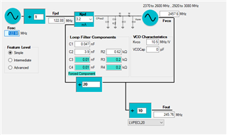
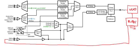
We are considering integrating the LMK04828 PLL into our design,
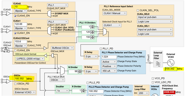
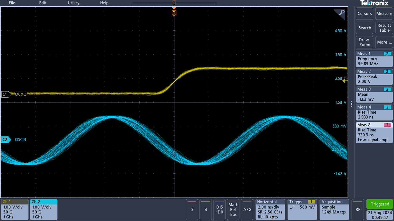
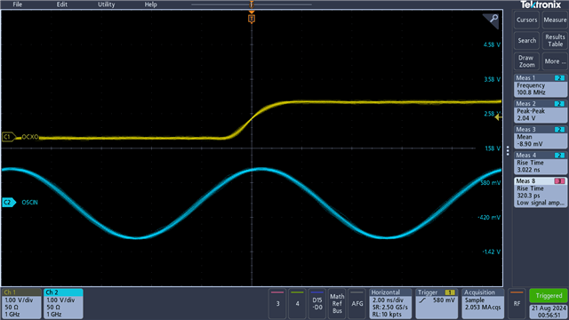
The goal of the PLL is to select one reference out of three 10MHz sinewave references and produce a 100MHz output.
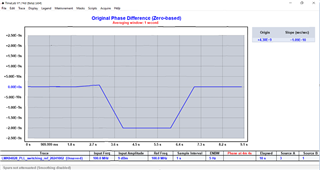
As the reference source is very clean and has low phase noise, we want to preserve the signal's phase noise.
Questions:
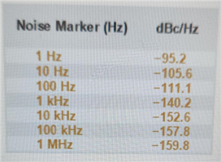
1) Are there phase noise measurements for the LMK04828 with 100MHz?
2) Are there any limitations to using a 10MHz sinewave as a reference input to the LMK04828?
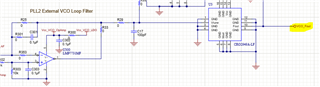
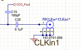
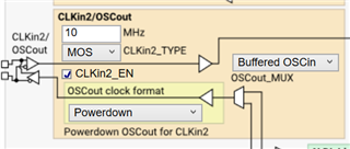
3) Can we replace the onboard VCXO with CVHD-950-100? It is footprint compatible.
4) Can we use the OSCIN (the VCXO output) as the PLL output? In that case, we use only PLL1
5) The LMK0482x family consists of more than one PLL. Based on the above requirements, how can we choose the best P/N?
6) The TICS Pro GUI for the LMK04828 supports .tcs file configurations. How do you prepare a configuration compatible with this file extension?
We have already tried using the Clock Design Tool and PLLatinum Sim, but both configuration files have different extensions and are not supported by the GUI.
email: alse@gmv.com
Thanks in advance,
Alon Sechan