- Ask a related questionWhat is a related question?A related question is a question created from another question. When the related question is created, it will be automatically linked to the original question.
This thread has been locked.
If you have a related question, please click the "Ask a related question" button in the top right corner. The newly created question will be automatically linked to this question.
Tool/software:
Hi,
We are considering integrating the LMK04828 PLL into our design,
The goal of the PLL is to select one reference out of three 10MHz sinewave references and produce a 100MHz output.
As the reference source is very clean and has low phase noise, we want to preserve the signal's phase noise.
Questions:
1) Are there phase noise measurements for the LMK04828 with 100MHz?
2) Are there any limitations to using a 10MHz sinewave as a reference input to the LMK04828?
3) Can we replace the onboard VCXO with CVHD-950-100? It is footprint compatible.
4) Can we use the OSCIN (the VCXO output) as the PLL output? In that case, we use only PLL1
5) The LMK0482x family consists of more than one PLL. Based on the above requirements, how can we choose the best P/N?
6) The TICS Pro GUI for the LMK04828 supports .tcs file configurations. How do you prepare a configuration compatible with this file extension?
We have already tried using the Clock Design Tool and PLLatinum Sim, but both configuration files have different extensions and are not supported by the GUI.
email: alse@gmv.com
Thanks in advance,
Alon Sechan
Hi Will,
I'm looking forward for your reply.
Currently we are using the PLLatinum Sim to create a configuration (please let me know if this is the correct tool to use)
We noticed that we are not able to configure the PLL1 loop BW. Only PLL2 can be configured. Depicted in the figure below.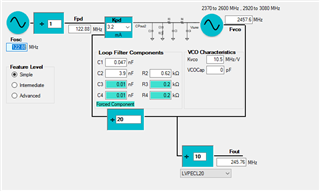
Could you please let us know how can we set the PLL1 loop BW. As per our design we don't use PLL2 (as our reference signal is very "clean").
Thanks,
Alon
Alon,
On the first screen you can select PLL1. I will answer the rest of you questions by tommorow.
Regards,
Will
Alon,
1) Are there phase noise measurements for the LMK04828 with 100MHz?
The phase noise will depend on the input and the configuration, so it can vary. Using PLLatinsim is the best way to estimate Phase Noise.
2) Are there any limitations to using a 10MHz sinewave as a reference input to the LMK04828?
No.
3) Can we replace the onboard VCXO with CVHD-950-100? It is footprint compatible.
Yes.
4) Can we use the OSCIN (the VCXO output) as the PLL output? In that case, we use only PLL1
Yes. In this case you would not need a VCXO for single loop mode.
5) The LMK0482x family consists of more than one PLL. Based on the above requirements, how can we choose the best P/N?
If your input clock signal is poor and you which to truly jitter clean, then Dual loop Mode will get the best performance. If your signal is already very low PN then single loop mode will also give good performance.
6) The TICS Pro GUI for the LMK04828 supports .tcs file configurations. How do you prepare a configuration compatible with this file extension? We have already tried using the Clock Design Tool and PLLatinum Sim, but both configuration files have different extensions and are not supported by the GUI.
Unfortunately, we do not have a way of bringing data from PLLatinumSim or CTA into TicsPro. As they are both graphical interfaces, I reccomend just bringing them side by side and copying the PLL settings into TicsPro as there are not many visible in PLLatinumSim anyways.
Regards,
Will
Hi Will,
Great! Thanks for the reply
Questions for clarification:
1) We don't find an option to select the VCXO P/N in the TICS Pro.
Should we only change the frequencies as depicted in the figure below?
We cannot put the exact value of 100MHz, the nearest value is 100.352MHz.
Also, the N Divider for OSCin is higher than expected. Both inputs to PLL1_PD should be with the same frequency, right?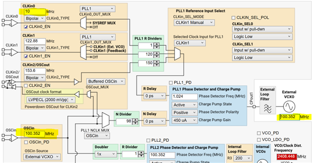
If I understand correctly, in TICS Pro we will configure and program the PLL. And PLLatinum Sim is a complementary tool to set the values of the PLL1 loop BW etc.?
2) As for choosing the right PLL P/N. There are LMK04821, LMK04826 and LMK04828. How to know which one to choose based on my requirements?
Thanks,
Alon
Alon,
Sorry for the delay.
1) The reason you cannot set the VCXO frequency correctly is because you have CLKin1 selected as your input so because 100MHz is not a multiple of a factor 122.88MHz it is not letting you set the VCXO to 100MHz. Change the Selected Clock Input for PLL1 to CLKin0 (10MHz)
If I understand correctly, in TICS Pro we will configure and program the PLL. And PLLatinum Sim is a complementary tool to set the values of the PLL1 loop BW etc.?
Yes, you are correct.
2) I am now confused what PLL P/N means, could you explain? The only difference is the VCO frequency, so depending on your output frequency you need a VCO frequency that can divide down to all of your desired output frequencies. Different VCO ranges on each device allow for different output frequency plans. There is no performance difference between them.
Regards,
Will
Hi Will,
For application we need lower phase noise (PN) as possible.
Our reference input PN is very low (coming directly from a maser source)
When measuring the LMK04828 PN we noticed that when using OSCout as output we receive lower PN than when using CLKout0 as output.
Our conclusion is that we should use PLL1 only and not use PLL2, as it only degrade the PN.
However, we need to use three input references in our design, therefore we need to use OSCout as CLKin2 input.
The other option is using OSCin as output, but we noticed it doesn't support a termination of 50Ohm (our phase noise analyser input impedance is a fixed 50 Ohm) it does supports 1MOhm but we cannot use it in our application.
What we are thinking to do next is:
1) To connect OSCin to an external buffer. For that we would like a recommendation for a suitablr low PN buffer.
2) Or we can fine tune the PLL loop BW.
Based on the above, can you suggest us action plan? Are we missing something? Please advise.
- We are using the LMK04828BEVM.
Thanks,
Alon
Alon,
I understand now.
PLL1 is going to have superior performance because it is using a VCXO which tend to have very good phase noise performance. PLL2 is using the internal VCO which is not as performant but it mainly used for generating a wide variety of clock frequencies as the VCO pulling range is in the GHz range.
If all you want to do is generate 100MHz outputs from your 10MHz output then the best solution would be to use PLL2, but select the external VCO option. Then you can connect your VCXO to CLKin1 and use PLL2 as your low noise 100MHz outputs. See the datasheet and TICSPro for more info on how to configure PLL2 is External VCO Mode.
Regards,
Will
Hi Will,
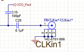
All of the components for the PLL2 external VCO are not mounted.
We can assemble them. But, as shown at the pictures below, by using the external VCO we will not be able to use CLKin1 as input.
We need to use all the three inputs for our design.
Can you please advise?
Thanks,
Alon
Hi Will,
1) Another way I thought to improve the PN is by changing the loop BW of PLL2.
Can you help me with identifying the components at the network of PLL2? I'm not sure how to map it.
The PLL2 loop network from the PLLatinum Sim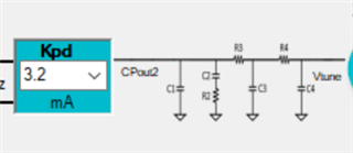
The PLL2 loop network from the LMK04828BEVM schematic.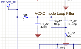
2) Can it be possible to use OSCin as our output? As we noticed that the OSCin cannot be used with a 50Ohm termination, can you suggest us a low PN buffer to be used with OSCin as output?
Looking forward for your reply.
Thanks,
Alon
Hello,
Sorry for the delay. I will try to get back to you tomorrow.
Regards,
Will
Hi Will,
We removed the 51Ohm resistor in parallel to the OSCin input, currently we are able to perform measurements at the OSCin connector.
The PN results are much better, except at 100Hz offset from the carrier frequency (the 100MHz). From the simulation results it should be -116 dBc/Hz, whereas we achieve -111dBc/Hz.
Can you advise how we can proceed to improve the PN at 100Hz away from the carrier?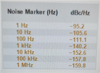
Additionally, the waveform shape from the OSCin output doesn't look square or sinewave, can you suggest us which buffer to use to get a square wave shape with low PN?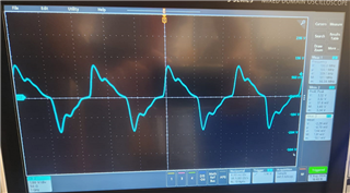
Thanks,
Alon
Alon,
Sorry for the delay. I am a little confused. Where are you taking your Phase Noise measurements? If it is from OSCout then you can program the output type to LVDS and use the oscilloscope to terminate each end to the internal 50 ohm termination. Doing the Math function difference between the two channels, you can see the effective differential signal. And if you are measuring from OSCout, what simulation are you referencing?
If you are measuring from somewhere else, please let me know where and I can better assist.
The signal distortion looks very likely to be a result of improper termination. Ensure both sides of a differential signal are properly terminated and that the termination is correct as shown in the datasheet. Once I know where you are measuring from, I can help with your optimization.
Regards,
Will
Hi Will,
All the measurements are taken at OSCin; I'm using it as the PLL's output. The reasoning is to achieve the lowest phase noise possible .
Looking forward to your reply.
Thanks,
Alon
Alon,
I understand. Measuring the VCXO output at OSCin will result in reflections due to the improper termination caused by the internal circuitry of OSCin on the same trace as where you are measuring with a 50 ohm termination with your scope. My guess is that you are seeing bad phase noise and the distorted scope capture because of how you are measuring it. If you can remove it from the osc in connection and measure it straight out of the VCXO this is how you will be able to see the true performance.
So just to confirm your requirements you need:
3 selectable inputs
Phase determinism between the input and the output
As you have suggested, I think we can do something like this with PLL1:
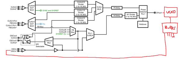
To follow up, how many outputs do you require, and what output type? I can recommend a buffer with your answer.
Regards,
Will
Hi Will,
Thank you for the reply.
We need one single-ended output.
Can you suggest a buffer?
Thanks,
Alon
Hi Will,
We are testing the manual switching of the LMK04828 clock inputs with the TICS pro GUI.
Switching between clkin0 and clkin1 works properly. But, when trying to switch to clkin2, the PLL's output is not completely locking to the clkin2 input
See the below the figures,
Unlocked condition: In yellow is the input to clkin2 and in blue the output from the PLL (The VCXO output filtered with a 100MHz LPF)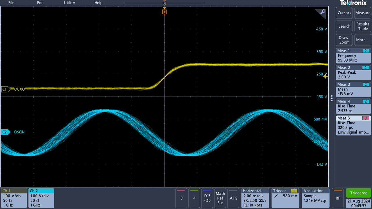
Locked condition: In yellow is the input to clkin0 and in blue the output from the PLL (The VCXO output filtered with a 100MHz LPF)
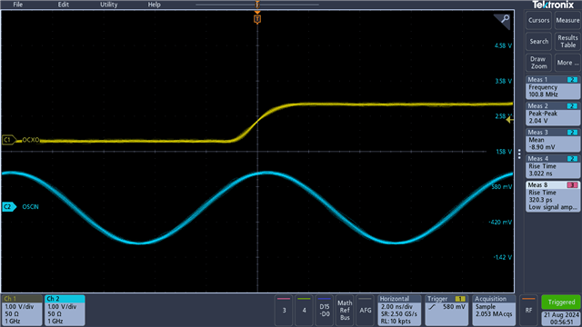
Thanks,
Alon
Alon,
Here a few things to check:
Let me know if these help with the locking and we can go from there.
Regards,
Will
Hi Will,
1) The switching issue was resolved, after we changed to clkin2* (the inverted input). We noticed that the PLL1 doesn't lock to clkin2 (non-inverted input).
2) We noticed that PLL1 is locking to clkin2* only when the input set to MOS. When it set to Bipolar the PLL1 doesn't lock to the clkin2* input.
After performing phase noise measurement to the PLL's output (OSCIN) we noticed that when we set the input to Bipolar the output phase noise is better than when we set it to MOS.
Can you advise? Is there any difference in the circuitry of clkin2* and the other inputs? When comparing between the different inputs, the phase noise results are the same when using clkin0 or clkin1, but is much different (worst) when we use clkin2*
Thanks,
Alon
Alon,
MOS will result in worse performance than the Bipolar input path. I was able to get Bipolar mode on CLKin2 by ensure the termination for CLKIN2 is correct and making sure that OSCout_FMT is set to Powerdown. If you are using the evm, you will need to rework CLKin2 for an input.
Regards,
Will
Hi Will,
I connected the 10MHz input to the CLKin2* (the inverting input) and CLKin2 (non-inverting input) is terminated with 50Ohm.
Additionally, the OSCout clock format is set to power down.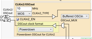
PLL1 is locked only when the CLKin2_TYPE is set to MOS. We cannot work with MOS as its phase noise performance is not sufficient for our requirements.
Can you please clarify what rework do I need to perform?
I'm working with the evaluation board.
Thanks,
Alon
Hi Will,
1) Can you please share your setup where the CLKin2 works with Bipolar input?
2) We measured the waveform at OSCout_N (left side of C24). it seems to be with 1V mean voltage.
Whereas for CLKin0 when we performed similar measurement (after the capacitor before the PLL pin) we measured a mean voltage of 1.5V.
Both have the same input signal.
- Why do we see this DC offset after the capacitor?
Please let me know if you need more information from my side.
Thanks,
Alon
Alon,
1) I configured CLKIn2/OSCout the same as the default CLKIn1 input as shown in the User Guide. As shown below:
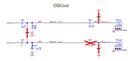

2) There is a bias voltage on each on the input pins, therefore after AC coupling there should be a measurable bias voltage, that might change depending on the termination scheme present after the ac coupling pins.
Let me know if you need anything else,
Will
Hi Will,
After configuring the CLKIn2/OSCout as per the photos you shared, it works—thank you!
However, we've encountered another issue. We're measuring phase noise from the OSCin output with a 10MHz reference connected to the CLKIn2 input. When a second 10MHz reference is connected to CLKIn0, and the PLL is locked to CLKIn2, the phase noise degrades significantly, suggesting interference from CLKIn0.
Could you advise on how to resolve this? In our design, we plan to use all three reference inputs with different 10MHz sources.
Thanks,
Alon
Hi Will,
I hope you're doing well.
I wanted to ask if there is any update regarding my previous message?
We've connected the same reference clock to both CLKin0 and CLKin2 using a splitter. We tested it on the oscilloscope and confirmed that there is no asymmetrical delay. The attached photo shows the phase difference between the reference and the PLL output (OSCin). We're observing a 2ns phase transition when switching between CLKin2 and CLKin0, and vice versa.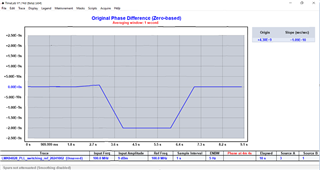
Could you confirm if there is a constant 2ns delay between these channels? Additionally, is there a way to adjust this delay in the GUI/registers?
Thanks for your help.
Best regards,
Alon Sechan
Thanks,
Alon
Alon,
Sorry for the delay. I am assigning this question to another apps engineer who is now covering this part. He will get back to you by tomorrow.
Regards,
Will
Hi,
I wanted to follow up on my previous questions and check if there’s an update.
Looking forward to hearing from you.
Thanks,
Alon
Hi Alon,
Sorry for my delay in getting to you. I am working towards answering your questions, but I have a question. You mentioned that you were measuring the phase noise and phase delay at the OSC_in pin. Can I ask why you are doing that? The OSC_in pin is only configured for an input.
Thanks,
Michael
Hi Michael,
I'm using OSCin as the VCXO output, and I've noticed that the phase noise results
have improved compared to PLL2 when using OSCin as the PLL output. in my configuration, PLL2 is powered down, and only PLL1 is active.
Thanks,
Alon
Hi Alon,
Thank you for your response. OSCin and the VCXO output are technically the same signal, but there are input terminations on the OSCin pin that make it unsuitable for directly measuring the output of the VCXO signal. This requires rework to the EVM that I will be happy to do next week. In the meantime, the STATUS_LDx pins can output the phase detector edges. Have you examined the STATUS_LDx pins with the outputs assigned to the PLL1 R and PLL1 N ports? If these edges also move by 2 ns upon input switching, then we can definitively know whether the issue occurring is the result of the phase detector or the traces.
Thanks,
Michael