This thread has been locked.

If you have a related question, please click the "Ask a related question" button in the top right corner. The newly created question will be automatically linked to this question.

LMX1214: AUXCLKOUT

Part Number: LMX1214

Tool/software:

Hi,

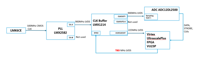
We have an implementation as below and a requirement to have a common clock source for both ADC sampling clock and FPGA.

Since FPGA cannot take 900MHz input (from CH-B of PLL or CLKOUTS2-4 of ClkBuffer), we plan to use 225MHz LVDS from AUXCLKOUT pins of clock buffer.

Per my understanding to sync the outputs of CLKOUT1 and AUXCLKOUT: SYNC pin is mandatory. 

1) Is that correct?

2) If yes, we are thinking of sending the SYNC input along with the clock buffer configuration settings which will be programmed thru' SPI at the start of the Clock buffer.

Can you pls confirm that ONE SYNC trigger is sufficient to be sent from FPGA at the buffer startup along with other SPI config settings?

3) Is there any frequency requirement for this SYNC LVDS trigger input to Clockbuffer?
Thanks

    1. SYNC is only required when any of the following conditions are true:

      1. Synchronizing multiple LMX1214 devices

      2. Synchronizing divided AUXCLKOUT to some other divided clock in the system (which isn't generated itself by AUXCLKOUT)
      3. Using main divider, and need AUXCLKOUT aligned with CLKOUT at a precise edge
    2. Supposing you did want to SYNC for any of the above reasons, one SYNC trigger at startup (after SPI configuration) is sufficient for normal operation. There are some fault conditions to consider, some of which may be handled in other ways (e.g. full system reset) or out of scope:
      1. Device loses power - register state is lost, divider state is lost, new SYNC would be required.
      2. Divider programming changes - divider state is lost, new SYNC would be required. In the absence of extreme interference (loss of power, operation substantially over or under recommended temperature/voltage, ionizing radiation, etc), divider programming only ever changes by intentional SPI write from the bus controller.
      3. Input clock is temporarily removed - divider state is preserved, but since some input cycles are missing, divider output is potentially at a new phase alignment. In the absence of extreme interference, the input clock chain should not spontaneously go away.
    3. There are two restrictions on the timing of signals sent to the SYNC:
      1. After the rising edge, the SYNC input must remain logic HIGH for 6 CLKIN clock cycles.
      2. At least 75 CLKIN clock cycles must occur between each rising edge on the SYNC input.
  • Hi Derek,

    Thanks for the details.

    Once this sync input signal is given as 'high' to the Clock buffer, can we keep it high until the next power cycle or until next SPI configuration? Or should it be periodic after certain number of clock cycles? 

    Nandini