This thread has been locked.

If you have a related question, please click the "Ask a related question" button in the top right corner. The newly created question will be automatically linked to this question.

CDCEL913: Unable to get desired output frequency

Part Number: CDCEL913
Other Parts Discussed in Thread: CDCE913, CLOCKPRO

Tool/software:

Dear Expert,

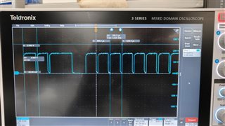
After generating the register values through TI's Clock Pro Software and programming the IC using ADB I am unable to generate the desired 63 MHz frequency.

Attached image below shows that I am only able to generate 3-4 KHz even though my input from crystal oscillator is 20 MHz.


  • Adarsh,

    Our team is currently out of office for the US holiday. Please expect a response by next Monday.

    Thanks,

    Kadeem

  • Adarsh,

    Please try using this configuration file:

    https://e2e.ti.com/cfs-file/__key/communityserver-discussions-components-files/48/CDCE913_5F00_20MHz_5F00_In_5F00_63MHz_5F00_Out.ISF

    Thanks,

    Kadeem

  • Dear Kadeem,

    The configuration file you shared does not seem to provide the desired frequency. I am observing a maximum output of 3-4 kHz. I am applying these values via I2C using ADB commands.

    Could you confirm if there is a specific sequence that needs to be followed during configuration? Any additional guidance would be greatly appreciated.

    Thank you for your support.

    Best regards,
    Adarsh

  • Adarsh,

    Are you using the EVM or a custom board? If the custom board, do you have it reworked to support an external clock on CLK_IN instead of the onboard XTAL?

    When using this exact file, I have no issues. I simply write the registers in order using ClockPro.

    Thanks,

    Kadeem

  • Dear Kadeem,

    We are using a custom board. Attached below is the schematic of the Reference clock circuit. We are tapping into the I2C lines and programming the IC.


  • Adarsh,

    So - if you set MUX1 to select PLL Bypass instead of the PLL output, are you seeing the 20MHz from the XTAL buffered out? If not, then the issue lies with the communication procedure.

    Are you able to send a register readback of the device settings?

    Thanks,

    Kadeem

  • Dear Kadeem,

    Even after setting MUX1 to PLL bypass, the observed waveforms remain unchanged. However, upon removing R240 and setting MUX1 to PLL bypass, we were able to generate a 20 MHz clock signal. Despite this, sending all the register values still does not produce the desired output.

    It seems the issue may be related to the script. Would you have a verified script or any suggestions that we could use to confirm the configuration settings?

    Thank you for your assistance.

    Best regards,
    Adarsh

  • Adarsh,

    We do not have any script or programming instructions outside of the configuration file from Clock Pro (attached).

    Getting the 20MHz signal means that the device is properly operating in buffer mode (the default).

    My recommendation would be to verify I2C connection at the device side by monitoring the SDA and SCL waveforms at the CDCE913 side.

    Alternatively, the CDCE913 evaluation module can be used to communicate with the device using Clock Pro by connecting the on-board SDA and SCL to your board instead of to the on-board CDCE913:

    The waveform from this method can be checked against your current register writing process to ensure that there are no issues.

    Thanks,
    Kadeem