This thread has been locked.

If you have a related question, please click the "Ask a related question" button in the top right corner. The newly created question will be automatically linked to this question.

TLK2711-SP: TLK2711-SP Clock Jitter

Part Number: TLK2711-SP
Other Parts Discussed in Thread: LMK00804B,

Tool/software:

Dear,

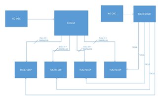
I'll use TLK-2711SP with kintex7 fpga like below figure.

Unfortunately, FPGA clocks have poor jitter characteristics. So, I think I will try to design it as shown in the picture below.

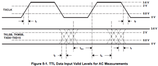
How can I match the timing of Clock and Data?

Best regards,

  • Hi Dean,

    TXCLK input should be synchronous with TXD data inputs because the rising edge of the clock signal is used to sample the data signals. Therefore I don't believe it is possible to use a second oscillator as the TXCLK input because it may drift away from the data signals' clock domain over time.

    Does the FPGA clock output meet these requirements? If it does, I recommend sticking with this design.

    If it doesn't, is it possible to buffer or split the same oscillator, externally from the FPGA? I'm assuming FPGA data outputs are synchronous with its reference clock input.

    Best,

    Lucas

  • The FPGA's Output Clock does not satisfy the jitter characteristics.Are there any other good options?

  • Hi Dean,

    My recommendation is to use a clock buffer to feed the same refclk input to the FPGA and to each TLK device. This is under the assumption that the FPGA data outputs are synchronous with its refclk input.

    Best,

    Lucas

  • When using a clock buffer, how do I resolve the delay due to pattern length and the buffer's skew?

  • Hi Dean,

    I'm looking into this and will get back to you shortly.

    Best,

    Lucas

  • Hi Dean,

    To get a better idea of clock buffer jitter and skew specs, I reviewed LMK00804B, a TI fanout buffer which I believe can be used with TLK2711-SP. This device has a typical additive jitter of 40 fs RMS, which is significantly smaller than the TLK reference clock jitter requirement of 40 ps p-p. Additionally, this device has a max propagation delay of 2.2 ns and max output skew of 35 ps. The max reference clock frequency of the TLK is 125 MHz, which is equivalent to a minimum period of 8 ns. This means the skew specs of the clock buffer should not negatively impact performance on the TLK. Since the TLK samples data signals on the rising edge of the reference clock, we simply need to ensure that data signals do not transition at the same time as the rising edge.

    Note that I am not an expert on clocking devices. If you have more detailed questions about TI's clocking and timing devices, please post a new E2E forum question and a responsible engineer will be assigned to your thread.

    I do have a few questions to confirm this type of design should work.

    • Is the XO OSC frequency the same as the FPGA data outputs?
    • Is the XO OSC synchronous with the FPGA data outputs?

    Best,

    Lucas

  • Thank you for the good idea.

    • Is the XO OSC frequency the same as the FPGA data outputs? Right. However, it goes through the logic buffer.
    • Is the XO OSC synchronous with the FPGA data outputs? if data is output from the FPGA and the clock is output from the clock buffer, how can the timing between the data and clock be matched?
  • Hi Dean,

    Thank you for your clarifications.

    Since the XO OSC output operates on the same clock domain as the FPGA data outputs, I believe the TLK should correctly sample all incoming data as long as the GTX_CLK input and the TX data inputs do not transition at the same time. Specifically, the t_su and t_h specs in the datasheet should be followed.

    It's likely necessary to design the layout very carefully and take timing measurements to ensure clock and data transitions do not happen at the same time.

    Best,

    Lucas

  • However, I can't control the timing of the clock buffer's output.

    when clock is output from FPGA, jitter occurs due to internal logic buffer.

    What should I do?

  • Hi Dean,

    I recommend creating another E2E thread with a clock/timing part number, as the clocking and timing team is better equipped to answer your questions. Another idea I have is to possibly use a jitter cleaner on the FPGA clock output.

    Best,

    Lucas

  • The category has been moved. Could you change the person?

  • Hi Dean,

    Please start a new thread with a part number such as LMK00804B and it will automatically be assigned to the correct person.

    Best,

    Lucas